ZHCSCK8G May 2014 – October 2017 LP8860-Q1
PRODUCTION DATA.
- 1 特性
- 2 应用
- 3 说明
- 4 修订历史记录
- 5 器件比较表
- 6 Pin Configuration and Functions
-
7 Specifications
- 7.1 Absolute Maximum Ratings
- 7.2 ESD Ratings
- 7.3 Recommended Operating Conditions
- 7.4 Thermal Information
- 7.5 Electrical Characteristics
- 7.6 Current Sinks Electrical Characteristics
- 7.7 Boost Converter Characteristics
- 7.8 Logic Interface Characteristics
- 7.9 VIN Undervoltage Protection (VIN_UVLO)
- 7.10 VDD Undervoltage Protection (VDD_UVLO)
- 7.11 VIN Overvoltage Protection (VIN_OVP)
- 7.12 VIN Overcurrent Protection (VIN_OCP)
- 7.13 Power-Line FET Control Electrical Characteristics
- 7.14 External Temp Sensor Control Electrical Characteristics
- 7.15 I2C Serial Bus Timing Parameters (SDA, SCLK)
- 7.16 SPI Timing Requirements
- 7.17 Typical Characteristics
-
8 Detailed Description
- 8.1 Overview
- 8.2 Functional Block Diagram
- 8.3 Feature Description
- 8.4 Device Functional Modes
- 8.5 Programming
- 8.6
Register Maps
- 8.6.1
Register Bit Explanations
- 8.6.1.1 Display/Cluster1 Brightness Control MSB
- 8.6.1.2 Display/Cluster1 Brightness Control LSB
- 8.6.1.3 Display/Cluster1 Output Current MSB
- 8.6.1.4 Display/Cluster1 Output Current LSB
- 8.6.1.5 Cluster2 Brightness Control MSB
- 8.6.1.6 Cluster2 Brightness Control LSB
- 8.6.1.7 Cluster2 Output Current
- 8.6.1.8 Cluster3 Brightness Control MSB
- 8.6.1.9 Cluster3 Brightness Control LSB
- 8.6.1.10 Cluster3 Output Current
- 8.6.1.11 Cluster4 Brightness Control MSB
- 8.6.1.12 Cluster4 Brightness Control LSB
- 8.6.1.13 Cluster4 Output Current
- 8.6.1.14 Configuration
- 8.6.1.15 Status
- 8.6.1.16 Fault
- 8.6.1.17 LED Fault
- 8.6.1.18 Fault Clear
- 8.6.1.19 Identification
- 8.6.1.20 Temp MSB
- 8.6.1.21 Temp LSB
- 8.6.1.22 Display LED Current MSB
- 8.6.1.23 Display LED Current LSB
- 8.6.1.24 Display LED PWM MSB
- 8.6.1.25 Display LED PWM LSB
- 8.6.1.26 EEPROM Control
- 8.6.1.27 EEPROM Unlock Code
- 8.6.2
EEPROM Bit Explanations
- 8.6.2.1 EEPROM Register 0
- 8.6.2.2 EEPROM Register 1
- 8.6.2.3 EEPROM Register 2
- 8.6.2.4 EEPROM Register 3
- 8.6.2.5 EEPROM Register 4
- 8.6.2.6 EEPROM Register 5
- 8.6.2.7 EEPROM Register 6
- 8.6.2.8 EEPROM Register 7
- 8.6.2.9 EEPROM Register 8
- 8.6.2.10 EEPROM Register 9
- 8.6.2.11 EEPROM Register 10
- 8.6.2.12 EEPROM Register 11
- 8.6.2.13 EEPROM Register 12
- 8.6.2.14 EEPROM Register 13
- 8.6.2.15 EEPROM Register 14
- 8.6.2.16 EEPROM Register 15
- 8.6.2.17 EEPROM Register 16
- 8.6.2.18 EEPROM Register 17
- 8.6.2.19 EEPROM Register 18
- 8.6.2.20 EEPROM Register 19
- 8.6.2.21 EEPROM Register 20
- 8.6.2.22 EEPROM Register 21
- 8.6.2.23 EEPROM Register 22
- 8.6.2.24 EEPROM Register 23
- 8.6.2.25 EEPROM Register 24
- 8.6.1
Register Bit Explanations
-
9 Application and Implementation
- 9.1 Application Information
- 9.2
Typical Applications
- 9.2.1
Typical Application for Display Backlight
- 9.2.1.1 Design Requirements
- 9.2.1.2
Detailed Design Procedure
- 9.2.1.2.1 Inductor Selection
- 9.2.1.2.2 Output Capacitor Selection
- 9.2.1.2.3 Input Capacitor Selection
- 9.2.1.2.4 Charge Pump Output Capacitor
- 9.2.1.2.5 Charge Pump Flying Capacitor
- 9.2.1.2.6 Diode
- 9.2.1.2.7 Boost Converter Transistor
- 9.2.1.2.8 Boost Sense Resistor
- 9.2.1.2.9 Power Line Transistor
- 9.2.1.2.10 Input Current Sense Resistor
- 9.2.1.2.11 Filter Component Values
- 9.2.1.3 Application Performance Plots
- 9.2.2 Low VDD Voltage and Combined Output Mode Application
- 9.2.3 High Output Voltage Application
- 9.2.4 High Output Current Application
- 9.2.5 Three-Channel Configuration Without Serial Interface
- 9.2.6 Solution With Minimum External Components
- 9.2.1
Typical Application for Display Backlight
- 10Power Supply Recommendations
- 11Layout
- 12器件和文档支持
- 13机械、封装和可订购信息
8.3.1.2 LED PWM Frequency and Resolution
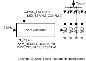
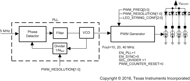
LED output PWM frequency is selected with <PWM_FREQ[3:0]> EEPROM register when using a 5-MHz internal oscillator for generating PWM output. <LED_STRING_CONF[2:0]> bits define phase shift between LED outputs as described later. <PWM_RESOLUTION[1:0]> EEPROM bits select the PLL output frequency and hence the LED PWM resolution. PWM frequencies with <EN_SYNC> = 0 are listed in Table 1.
NOTE
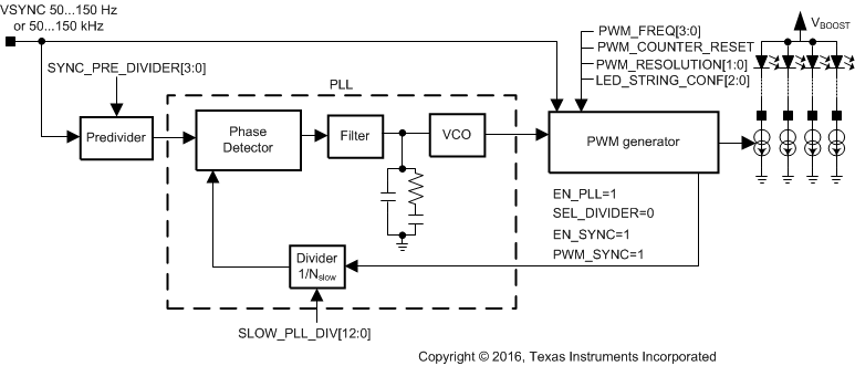
If the VSYNC signal is used for generating PWM output frequency, it affects all clock frequencies, as well as the LED PWM output frequency. The EEPROM Bit Explanations section explains how all the dividers affect the output clocks.
 Figure 10. PWM Clocking With Internal Oscillator
 Figure 11. PWM Clocking With PLL, Internal Oscillator as Reference
Table 1. Output PWM Frequency and Resolution With Internal Oscillator
| 00
OSC = 5 MHz |
01
OSC = 10 MHz |
10
OSC = 20 MHz |
11
OSC = 40 MHz |
||
|---|---|---|---|---|---|
| PWM_FREQ[3:0] | PWM_RESOLUTION[1:0]
PWM FREQUENCY (Hz) |
RESOLUTION (bit) | |||
| 1111 | 39063 | 7 | 8 | 9 | 10 |
| 1110 | 34180 | 7 | 8 | 9 | 10 |
| 1101 | 30518 | 7 | 8 | 9 | 10 |
| 1100 | 29297 | 7 | 8 | 9 | 10 |
| 1011 | 28076 | 7 | 8 | 9 | 10 |
| 1010 | 26855 | 7 | 8 | 9 | 10 |
| 1001 | 25635 | 7 | 8 | 9 | 10 |
| 1000 | 24412 | 7 | 8 | 9 | 10 |
| 0111 | 23192 | 7 | 8 | 9 | 10 |
| 0110 | 21973 | 7 | 8 | 9 | 10 |
| 0101 | 20752 | 7 | 8 | 9 | 10 |
| 0100 | 19531 | 8 | 9 | 10 | 11 |
| 0011 | 17090 | 8 | 9 | 10 | 11 |
| 0010 | 13428 | 8 | 9 | 10 | 11 |
| 0001 | 9766 | 9 | 10 | 11 | 12 |
| 0000 | 4883 | 10 | 11 | 12 | 13 |
 Figure 12. PWM Synchronization With External VSYNC Input
PWM clock frequencies with different <SEL_DIVIDER>, <EN_PLL>, and <EN_SYNC> combinations are listed in Table 2.
Table 2. PLL Clock and LED PWM Frequency
| PWM_SYNC | SEL_DIVIDER | EN_PLL | EN_SYNC | PLL CLOCK | PWM FREQUENCY |
|---|---|---|---|---|---|
| 0 | X | 0 | 0 | 5 MHz | See Table 1 |
| 0 | 1 | 1 | 0 | 5, 10, 20, 40 MHz | See Table 1 |
| 0 | 0 | 1 | 1 | SYNC × R_SEL[1:0] × SLOW_PLL_DIV[12:0]/
SYNC_PRE_DIV[3:0] |
PLL clock / GEN_DIV |
| 1 | 0 | 1 | 1 | SYNC × GEN_DIV × SLOW_PLL_DIV[12:0]/
SYNC_PRE_DIV[3:0] |
PLL clock / GEN_DIV |
GEN_DIV coefficients and resolution (bit) are listed on Table 3.
Table 3. GEN_DIV Coefficients and Resolution
| PWM_RESOLUTION[1:0] | ||||||||||||
|---|---|---|---|---|---|---|---|---|---|---|---|---|
| 00 | 01 | 10 | 11 | |||||||||
| PWM_
FREQ[3:0] |
STEP | GEN_DIV | RES
(bits) |
STEP | GEN_DIV | RES
(bits) |
STEP | GEN_DIV | RES
(bits) |
STEP | GEN_DIV | RES
(bits) |
| 0000 | 64 | 1024.00 | 10 | 32 | 2048.00 | 11 | 16 | 4096.00 | 12 | 8 | 8192.00 | 13 |
| 0001 | 128 | 512.00 | 9 | 64 | 1024.00 | 10 | 32 | 2048.00 | 11 | 16 | 4096.00 | 12 |
| 0010 | 176 | 372.36 | 8 | 88 | 744.73 | 9 | 44 | 1489.45 | 10 | 22 | 2978.91 | 11 |
| 0011 | 224 | 292.57 | 8 | 112 | 585.14 | 9 | 56 | 1170.29 | 10 | 28 | 2340.57 | 11 |
| 0100 | 256 | 256.00 | 8 | 128 | 512.00 | 9 | 64 | 1024.00 | 10 | 32 | 2048.00 | 11 |
| 0101 | 272 | 240.94 | 7 | 136 | 481.88 | 8 | 68 | 963.76 | 9 | 34 | 1927.53 | 10 |
| 0110 | 288 | 227.56 | 7 | 144 | 455.11 | 8 | 72 | 910.22 | 9 | 36 | 1820.44 | 10 |
| 0111 | 304 | 215.58 | 7 | 152 | 431.16 | 8 | 76 | 862.32 | 9 | 38 | 1724.63 | 10 |
| 1000 | 320 | 204.80 | 7 | 160 | 409.60 | 8 | 80 | 819.20 | 9 | 40 | 1638.40 | 10 |
| 1001 | 336 | 195.05 | 7 | 168 | 390.10 | 8 | 84 | 780.19 | 9 | 42 | 1560.38 | 10 |
| 1010 | 352 | 186.18 | 7 | 176 | 372.36 | 8 | 88 | 744.73 | 9 | 44 | 1489.45 | 10 |
| 1011 | 368 | 178.09 | 7 | 184 | 356.17 | 8 | 92 | 712.35 | 9 | 46 | 1424.70 | 10 |
| 1100 | 384 | 170.67 | 7 | 192 | 341.33 | 8 | 96 | 682.67 | 9 | 48 | 1365.33 | 10 |
| 1101 | 400 | 163.84 | 7 | 200 | 327.68 | 8 | 100 | 655.36 | 9 | 50 | 1310.72 | 10 |
| 1110 | 448 | 146.29 | 7 | 224 | 292.57 | 8 | 112 | 585.14 | 9 | 56 | 1170.29 | 10 |
| 1111 | 512 | 128.00 | 7 | 256 | 256.00 | 8 | 128 | 512.00 | 9 | 64 | 1024.00 | 10 |
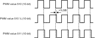
Dithering allows increased resolution and smaller average steps size. Dithering can be programmed with EEPROM bits <DITHER[2:0]> 0 to 4 bits. Figure 13 shows 1-bit dithering. For 3-bit dithering, every 8th pulse is made 1 LSB longer to increase the average value by 1/8th. Dither is available in steady state condition when <EN_STEADY_DITHER> is high, otherwise during slope only.
 Figure 13. Example of the Dithering, 1-Bit Dither, 10-Bit Resolution