ZHCSCK8G May 2014 – October 2017 LP8860-Q1
PRODUCTION DATA.
- 1 特性
- 2 应用
- 3 说明
- 4 修订历史记录
- 5 器件比较表
- 6 Pin Configuration and Functions
-
7 Specifications
- 7.1 Absolute Maximum Ratings
- 7.2 ESD Ratings
- 7.3 Recommended Operating Conditions
- 7.4 Thermal Information
- 7.5 Electrical Characteristics
- 7.6 Current Sinks Electrical Characteristics
- 7.7 Boost Converter Characteristics
- 7.8 Logic Interface Characteristics
- 7.9 VIN Undervoltage Protection (VIN_UVLO)
- 7.10 VDD Undervoltage Protection (VDD_UVLO)
- 7.11 VIN Overvoltage Protection (VIN_OVP)
- 7.12 VIN Overcurrent Protection (VIN_OCP)
- 7.13 Power-Line FET Control Electrical Characteristics
- 7.14 External Temp Sensor Control Electrical Characteristics
- 7.15 I2C Serial Bus Timing Parameters (SDA, SCLK)
- 7.16 SPI Timing Requirements
- 7.17 Typical Characteristics
-
8 Detailed Description
- 8.1 Overview
- 8.2 Functional Block Diagram
- 8.3 Feature Description
- 8.4 Device Functional Modes
- 8.5 Programming
- 8.6
Register Maps
- 8.6.1
Register Bit Explanations
- 8.6.1.1 Display/Cluster1 Brightness Control MSB
- 8.6.1.2 Display/Cluster1 Brightness Control LSB
- 8.6.1.3 Display/Cluster1 Output Current MSB
- 8.6.1.4 Display/Cluster1 Output Current LSB
- 8.6.1.5 Cluster2 Brightness Control MSB
- 8.6.1.6 Cluster2 Brightness Control LSB
- 8.6.1.7 Cluster2 Output Current
- 8.6.1.8 Cluster3 Brightness Control MSB
- 8.6.1.9 Cluster3 Brightness Control LSB
- 8.6.1.10 Cluster3 Output Current
- 8.6.1.11 Cluster4 Brightness Control MSB
- 8.6.1.12 Cluster4 Brightness Control LSB
- 8.6.1.13 Cluster4 Output Current
- 8.6.1.14 Configuration
- 8.6.1.15 Status
- 8.6.1.16 Fault
- 8.6.1.17 LED Fault
- 8.6.1.18 Fault Clear
- 8.6.1.19 Identification
- 8.6.1.20 Temp MSB
- 8.6.1.21 Temp LSB
- 8.6.1.22 Display LED Current MSB
- 8.6.1.23 Display LED Current LSB
- 8.6.1.24 Display LED PWM MSB
- 8.6.1.25 Display LED PWM LSB
- 8.6.1.26 EEPROM Control
- 8.6.1.27 EEPROM Unlock Code
- 8.6.2
EEPROM Bit Explanations
- 8.6.2.1 EEPROM Register 0
- 8.6.2.2 EEPROM Register 1
- 8.6.2.3 EEPROM Register 2
- 8.6.2.4 EEPROM Register 3
- 8.6.2.5 EEPROM Register 4
- 8.6.2.6 EEPROM Register 5
- 8.6.2.7 EEPROM Register 6
- 8.6.2.8 EEPROM Register 7
- 8.6.2.9 EEPROM Register 8
- 8.6.2.10 EEPROM Register 9
- 8.6.2.11 EEPROM Register 10
- 8.6.2.12 EEPROM Register 11
- 8.6.2.13 EEPROM Register 12
- 8.6.2.14 EEPROM Register 13
- 8.6.2.15 EEPROM Register 14
- 8.6.2.16 EEPROM Register 15
- 8.6.2.17 EEPROM Register 16
- 8.6.2.18 EEPROM Register 17
- 8.6.2.19 EEPROM Register 18
- 8.6.2.20 EEPROM Register 19
- 8.6.2.21 EEPROM Register 20
- 8.6.2.22 EEPROM Register 21
- 8.6.2.23 EEPROM Register 22
- 8.6.2.24 EEPROM Register 23
- 8.6.2.25 EEPROM Register 24
- 8.6.1
Register Bit Explanations
-
9 Application and Implementation
- 9.1 Application Information
- 9.2
Typical Applications
- 9.2.1
Typical Application for Display Backlight
- 9.2.1.1 Design Requirements
- 9.2.1.2
Detailed Design Procedure
- 9.2.1.2.1 Inductor Selection
- 9.2.1.2.2 Output Capacitor Selection
- 9.2.1.2.3 Input Capacitor Selection
- 9.2.1.2.4 Charge Pump Output Capacitor
- 9.2.1.2.5 Charge Pump Flying Capacitor
- 9.2.1.2.6 Diode
- 9.2.1.2.7 Boost Converter Transistor
- 9.2.1.2.8 Boost Sense Resistor
- 9.2.1.2.9 Power Line Transistor
- 9.2.1.2.10 Input Current Sense Resistor
- 9.2.1.2.11 Filter Component Values
- 9.2.1.3 Application Performance Plots
- 9.2.2 Low VDD Voltage and Combined Output Mode Application
- 9.2.3 High Output Voltage Application
- 9.2.4 High Output Current Application
- 9.2.5 Three-Channel Configuration Without Serial Interface
- 9.2.6 Solution With Minimum External Components
- 9.2.1
Typical Application for Display Backlight
- 10Power Supply Recommendations
- 11Layout
- 12器件和文档支持
- 13机械、封装和可订购信息
8.3.5 Cluster Mode
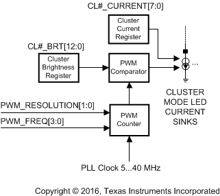
Cluster is a simplified mode which allows independent current and PWM control for every string in cluster mode. In this mode brightness control is limited to conventional PWM through the SPI/I2C brightness registers. The PWM input pin, Hybrid PWM and Current dimming mode, slope control, or dither are not available. Brightness for different LED strings depends on <DISP_CL1_BRT[15:0]>, <CL2_BRT[12:0]>, <CL3_BRT[12:0]> and <CL4_BRT[12:0]> registers. If OUT1 is in cluster mode, only 13 MSB are used. If all LED outputs are in the cluster mode, LED output PWM resolution is always 13 bits, and frequency depends on <PWM_RESOLUTION[1:0]> bits (see Table 13). If one or more of the LED outputs is in display mode, frequency, and resolution for strings in the cluster mode is the same as for strings in the display mode (see Table 1).
 Figure 20. Cluster Mode Block Diagram
Table 13. Output PWM Frequency for Mode 7 (All Strings in Cluster Mode)
| PWM_RESOLUTION[1:0] | 00 | 01 | 10 | 11 |
|---|---|---|---|---|
| OSC frequency (MHz) | 5 | 10 | 20 | 40 |
| ƒLED PWM (Hz) | 610 | 1221 | 2442 | 4883 |
When the LP8860-Q1 is set in cluster mode, fault protection functionality is limited. Headroom for LED strings must be between the high-voltage comparator level <DRV_LED_FAULT_THR[1:0]> and low-voltage comparator level <DRV_HEADR[2:0]> (which depend upon saturation voltage); otherwise a fault is generated.
Adaptive boost control does not follow strings in cluster mode. Display mode strings and cluster mode strings must not be connected to the same boost. When LED strings in display and cluster modes are connected to the same boost, LED open or short faults may be generated if the LED forward-voltage mismatch is too high.
If all LED outputs are in cluster mode, boost output voltage is fixed and must be set by EEPROM <BOOST_INITIAL_VOLTAGE[5:0]> bits to a value high enough to ensure correct LED string operation in all conditions.
<EN_CL_LED_FAULT>=0 disables cluster LED fault detection, even if all LED strings are in the cluster mode. The current de-rating (based on the internal temperature sensor) and LED current limitation (based on external temperature sensor) are not functional in this mode, and analog current dimming based on the external sensor functionality is limited (LED shutdown for high temperature is not operational).