ZHCSCK8G May 2014 – October 2017 LP8860-Q1
PRODUCTION DATA.
- 1 特性
- 2 应用
- 3 说明
- 4 修订历史记录
- 5 器件比较表
- 6 Pin Configuration and Functions
-
7 Specifications
- 7.1 Absolute Maximum Ratings
- 7.2 ESD Ratings
- 7.3 Recommended Operating Conditions
- 7.4 Thermal Information
- 7.5 Electrical Characteristics
- 7.6 Current Sinks Electrical Characteristics
- 7.7 Boost Converter Characteristics
- 7.8 Logic Interface Characteristics
- 7.9 VIN Undervoltage Protection (VIN_UVLO)
- 7.10 VDD Undervoltage Protection (VDD_UVLO)
- 7.11 VIN Overvoltage Protection (VIN_OVP)
- 7.12 VIN Overcurrent Protection (VIN_OCP)
- 7.13 Power-Line FET Control Electrical Characteristics
- 7.14 External Temp Sensor Control Electrical Characteristics
- 7.15 I2C Serial Bus Timing Parameters (SDA, SCLK)
- 7.16 SPI Timing Requirements
- 7.17 Typical Characteristics
-
8 Detailed Description
- 8.1 Overview
- 8.2 Functional Block Diagram
- 8.3 Feature Description
- 8.4 Device Functional Modes
- 8.5 Programming
- 8.6
Register Maps
- 8.6.1
Register Bit Explanations
- 8.6.1.1 Display/Cluster1 Brightness Control MSB
- 8.6.1.2 Display/Cluster1 Brightness Control LSB
- 8.6.1.3 Display/Cluster1 Output Current MSB
- 8.6.1.4 Display/Cluster1 Output Current LSB
- 8.6.1.5 Cluster2 Brightness Control MSB
- 8.6.1.6 Cluster2 Brightness Control LSB
- 8.6.1.7 Cluster2 Output Current
- 8.6.1.8 Cluster3 Brightness Control MSB
- 8.6.1.9 Cluster3 Brightness Control LSB
- 8.6.1.10 Cluster3 Output Current
- 8.6.1.11 Cluster4 Brightness Control MSB
- 8.6.1.12 Cluster4 Brightness Control LSB
- 8.6.1.13 Cluster4 Output Current
- 8.6.1.14 Configuration
- 8.6.1.15 Status
- 8.6.1.16 Fault
- 8.6.1.17 LED Fault
- 8.6.1.18 Fault Clear
- 8.6.1.19 Identification
- 8.6.1.20 Temp MSB
- 8.6.1.21 Temp LSB
- 8.6.1.22 Display LED Current MSB
- 8.6.1.23 Display LED Current LSB
- 8.6.1.24 Display LED PWM MSB
- 8.6.1.25 Display LED PWM LSB
- 8.6.1.26 EEPROM Control
- 8.6.1.27 EEPROM Unlock Code
- 8.6.2
EEPROM Bit Explanations
- 8.6.2.1 EEPROM Register 0
- 8.6.2.2 EEPROM Register 1
- 8.6.2.3 EEPROM Register 2
- 8.6.2.4 EEPROM Register 3
- 8.6.2.5 EEPROM Register 4
- 8.6.2.6 EEPROM Register 5
- 8.6.2.7 EEPROM Register 6
- 8.6.2.8 EEPROM Register 7
- 8.6.2.9 EEPROM Register 8
- 8.6.2.10 EEPROM Register 9
- 8.6.2.11 EEPROM Register 10
- 8.6.2.12 EEPROM Register 11
- 8.6.2.13 EEPROM Register 12
- 8.6.2.14 EEPROM Register 13
- 8.6.2.15 EEPROM Register 14
- 8.6.2.16 EEPROM Register 15
- 8.6.2.17 EEPROM Register 16
- 8.6.2.18 EEPROM Register 17
- 8.6.2.19 EEPROM Register 18
- 8.6.2.20 EEPROM Register 19
- 8.6.2.21 EEPROM Register 20
- 8.6.2.22 EEPROM Register 21
- 8.6.2.23 EEPROM Register 22
- 8.6.2.24 EEPROM Register 23
- 8.6.2.25 EEPROM Register 24
- 8.6.1
Register Bit Explanations
-
9 Application and Implementation
- 9.1 Application Information
- 9.2
Typical Applications
- 9.2.1
Typical Application for Display Backlight
- 9.2.1.1 Design Requirements
- 9.2.1.2
Detailed Design Procedure
- 9.2.1.2.1 Inductor Selection
- 9.2.1.2.2 Output Capacitor Selection
- 9.2.1.2.3 Input Capacitor Selection
- 9.2.1.2.4 Charge Pump Output Capacitor
- 9.2.1.2.5 Charge Pump Flying Capacitor
- 9.2.1.2.6 Diode
- 9.2.1.2.7 Boost Converter Transistor
- 9.2.1.2.8 Boost Sense Resistor
- 9.2.1.2.9 Power Line Transistor
- 9.2.1.2.10 Input Current Sense Resistor
- 9.2.1.2.11 Filter Component Values
- 9.2.1.3 Application Performance Plots
- 9.2.2 Low VDD Voltage and Combined Output Mode Application
- 9.2.3 High Output Voltage Application
- 9.2.4 High Output Current Application
- 9.2.5 Three-Channel Configuration Without Serial Interface
- 9.2.6 Solution With Minimum External Components
- 9.2.1
Typical Application for Display Backlight
- 10Power Supply Recommendations
- 11Layout
- 12器件和文档支持
- 13机械、封装和可订购信息
8.5.1 EEPROM
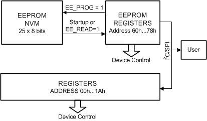
EEPROM memory stores various parameters for chip control. The 200-bit EEPROM memory is organized as 25 × 8 bits. The EEPROM structure consists of a register front-end and the non-volatile memory (NVM). Register data can be read and written through the I2C/SPI serial interface. EEPROM must be burned with the new data; otherwise, data disappears after power-on reset or VDDIO/EN cycling. PWM outputs and PLL must be disabled when writing to EEPROM registers or burning EEPROM (<DISP_CL1_BRT[15:0]> = 0, <CL2_BRT[12:0]> = 0, <CL3_BRT[12:0]> = 0, <CL2_BRT[12:0]> = 0, <EN_PLL> = 0). To read and program EEPROM NVM separate commands need to be sent. Erase and program voltages are generated internally; no other voltages other than the normal VDD voltage is required. A complete EEPROM memory map is shown in the Table 23.
The user must make sure that VDD power is on, and the VDDIO/EN pin is kept high, during the whole programming/burn sequence to avoid memory corruption.
 Figure 44. EEPROM and Register Configuration
EEPROM has protection against accidental writes. EEPROM access can be unlocked by writing a pass code to the EEPROM_UNLOCK register. It unlocks the EEPROM Control register EEPROM_CNTRL and all EEPROM registers. Lock is enabled again by writing any other code to the EEPROM_UNLOCK register (for example, 0x00 enables the lock any time).
Table 19. EEPROM Pass Code Protection
| PASS CODE TO EEPROM_UNLOCK REGISTER |
|---|
| 0x08, 0xBA, 0xEF |
EEPROM is used as fixed product-configuration storage, to be set or programmed during production before normal operation. EEPROM can be reprogrammed for evaluation purposes up to 1000 cycles. Data-retention lifetime for factory-programmed content is 10 years, minimum. For more details regarding EEPROM options, see TI Application Note Selecting the Correct LP8860-Q1 EEPROM Version (SNVA757).