ZHCSLM3B August 2020 – May 2024 LP8864-Q1
PRODUCTION DATA
- 1
- 1 特性
- 2 应用
- 3 说明
- 4 Pin Configuration and Functions
- 5 Specifications
-
6 Detailed Description
- 6.1 Overview
- 6.2 Functional Block Diagram
- 6.3
Feature Description
- 6.3.1 Control Interface
- 6.3.2 Function Setting
- 6.3.3 Device Supply (VDD)
- 6.3.4 Enable (EN)
- 6.3.5 Charge Pump
- 6.3.6 Boost Controller
- 6.3.7 LED Current Sinks
- 6.3.8 Brightness Control
- 6.3.9
Protection and Fault Detections
- 6.3.9.1 Supply Faults
- 6.3.9.2
Boost Faults
- 6.3.9.2.1 Boost Overvoltage Faults (BSTOVPL, BSTOVPH)
- 6.3.9.2.2 Boost Overcurrent Faults (BSTOCP)
- 6.3.9.2.3 LEDSET Resistor Missing Faults (LEDSET)
- 6.3.9.2.4 MODE Resistor Missing Faults (MODESEL)
- 6.3.9.2.5 FSET Resistor Missing Faults (FSET)
- 6.3.9.2.6 ISET Resistor Out of Range Faults (ISET)
- 6.3.9.2.7 Thermal Shutdown Faults (TSD)
- 6.3.9.3 LED Faults
- 6.3.9.4 Overview of the Fault and Protection Schemes
- 6.4 Device Functional Modes
- 6.5 Programming
-
7 Application and Implementation
- 7.1 Application Information
- 7.2
Typical Applications
- 7.2.1
Full Feature Application for Display Backlight
- 7.2.1.1 Design Requirements
- 7.2.1.2
Detailed Design Procedure
- 7.2.1.2.1 Inductor Selection
- 7.2.1.2.2 Output Capacitor Selection
- 7.2.1.2.3 Input Capacitor Selection
- 7.2.1.2.4 Charge Pump Output Capacitor
- 7.2.1.2.5 Charge Pump Flying Capacitor
- 7.2.1.2.6 Output Diode
- 7.2.1.2.7 Switching FET
- 7.2.1.2.8 Boost Sense Resistor
- 7.2.1.2.9 Power-Line FET
- 7.2.1.2.10 Input Current Sense Resistor
- 7.2.1.2.11 Feedback Resistor Divider
- 7.2.1.2.12 Critical Components for Design
- 7.2.1.3 Application Curves
- 7.2.2 Application with Basic/Minimal Operation
- 7.2.3
SEPIC Mode Application
- 7.2.3.1 Design Requirements
- 7.2.3.2
Detailed Design Procedure
- 7.2.3.2.1 Inductor Selection
- 7.2.3.2.2 Coupling Capacitor Selection
- 7.2.3.2.3 Output Capacitor Selection
- 7.2.3.2.4 Input Capacitor Selection
- 7.2.3.2.5 Charge Pump Output Capacitor
- 7.2.3.2.6 Charge Pump Flying Capacitor
- 7.2.3.2.7 Switching FET
- 7.2.3.2.8 Output Diode
- 7.2.3.2.9 Switching Sense Resistor
- 7.2.3.2.10 Power-Line FET
- 7.2.3.2.11 Input Current Sense Resistor
- 7.2.3.2.12 Feedback Resistor Divider
- 7.2.3.2.13 Critical Components for Design
- 7.2.3.3 Application Curves
- 7.2.1
Full Feature Application for Display Backlight
- 7.3 Power Supply Recommendations
- 7.4 Layout
- 8 Register Maps
- 9 Device and Documentation Support
- 10Revision History
- 11Mechanical, Packaging, and Orderable Information
封装选项
机械数据 (封装 | 引脚)
散热焊盘机械数据 (封装 | 引脚)
订购信息
7.2.1.2.12 Critical Components for Design
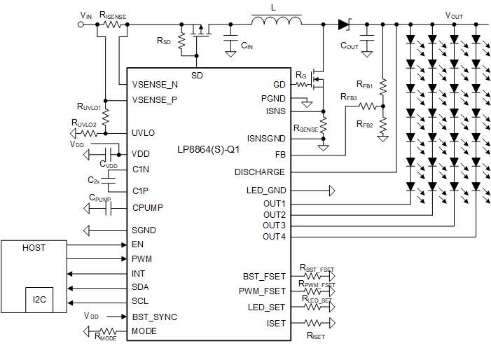
Figure 7-2 shows the critical part of circuitry: boost components, the LP8864-Q1 internal charge pump for gate-driver powering, and powering/grounding of LP8864-Q1 . Schematic example is shown in Figure 7-2.
 Figure 7-2 Critical Components for Full Feature
Design
Figure 7-2 Critical Components for Full Feature
DesignTable 7-3 Recommended Component Values for Full Feature Design Example
| REFERENCE DESIGNATOR | DESCRIPTION | NOTE |
|---|---|---|
| RISENSE | 20 mΩ, 3 W | Input current sensing resistor |
| RSD | 20 kΩ, 0.1 W | Power-line FET gate pullup resistor |
| RSENSE | 30mΩ, 3W | Boost current sensing resistor |
| RG | 15Ω, 0.1W | Gate resistor to control the rising/falling time of nMOSFET for EMC |
| RUVLO1 | 76.8kΩ, 0.1W | These UVLO resistor settings set the VIN_UVLO rising voltage at 3.75V, VIN_UVLO falling voltage at 3.35V |
| RUVLO2 | 20.5kΩ, 0.1W | |
| RFB3 | 0Ω, 0.1W | Not needed unless 100kΩ restrictions on resistors |
| RFB2 | 100kΩ, 0.1W | Bottom feedback divider resistor |
| RFB1 | 910kΩ, 0.1W | Top feedback divider resistor |
| RBST_FSET | 3.92kΩ, 0.1W | Boost frequency set resistor (400kHz) |
| RISET | 20.8kΩ, 0.1W | Current set resistor (150mA per channel) |
| RPWM_FSET | 17.8kΩ, 0.1W | Output PWM frequency set resistor (4.88kHz PWM frequency to avoid audible noise) |
| RMODE | 3.92kΩ, 0.1W | Mode resistor (Phase-Shift PWM mode with 0x3B I2C address) |
| RLED_SET | 3.92kΩ, 0.1W | LED_SET resistor (4channels configuration) |
| CPUMP | 10µF, 10V ceramic | Charge-pump output capacitor |
| C2X | 2.2µF, 10V ceramic | Flying capacitor |
| CVDD | 4.7µF + 0.1µF, 10V ceramic | VDD bypass capacitor |
| CIN | 1 × 33µF, 50V electrolytic + 1 × 10µF, 50V ceramic | Boost input capacitor |
| COUT | 1 × 33µF, 50V electrolytic + 1 × 10µF, 50V ceramic | Boost output capacitor |
| L1 | 22μH saturation current 6.5A | Boost inductor |
| D1 | 50V, 6.5A Schottky diode | Boost Schottky diode |
| Q1 | 60V, 15A nMOSFET | Boost nMOSFET |
| Q2 | 60V, 15A pMOSFET | Power-line FET |