ZHCSLM9B August 2020 – May 2024 LP8866S-Q1
PRODUCTION DATA
- 1
- 1 特性
- 2 应用
- 3 说明
- 4 Pin Configuration and Functions
- 5 Specifications
-
6 Detailed Description
- 6.1 Overview
- 6.2 Functional Block Diagram
- 6.3
Feature Description
- 6.3.1 Control Interface
- 6.3.2 Function Setting
- 6.3.3 Device Supply (VDD)
- 6.3.4 Enable (EN)
- 6.3.5 Charge Pump
- 6.3.6 Boost Controller
- 6.3.7 LED Current Sinks
- 6.3.8 Brightness Control
- 6.3.9
Protection and Fault Detections
- 6.3.9.1 Supply Faults
- 6.3.9.2
Boost Faults
- 6.3.9.2.1 Boost Overvoltage Faults (BSTOVPL, BSTOVPH)
- 6.3.9.2.2 Boost Overcurrent Faults (BSTOCP)
- 6.3.9.2.3 LEDSET Resistor Missing Faults (LEDSET)
- 6.3.9.2.4 MODE Resistor Missing Faults (MODESEL)
- 6.3.9.2.5 FSET Resistor Missing Faults (FSET)
- 6.3.9.2.6 ISET Resistor Out of Range Faults (ISET)
- 6.3.9.2.7 Thermal Shutdown Faults (TSD)
- 6.3.9.3 LED Faults
- 6.3.9.4 Overview of the Fault and Protection Schemes
- 6.4 Device Functional Modes
- 6.5 Programming
-
7 Application and Implementation
- 7.1 Application Information
- 7.2
Typical Applications
- 7.2.1
Full Feature Application for Display Backlight
- 7.2.1.1 Design Requirements
- 7.2.1.2
Detailed Design Procedure
- 7.2.1.2.1 Inductor Selection
- 7.2.1.2.2 Output Capacitor Selection
- 7.2.1.2.3 Input Capacitor Selection
- 7.2.1.2.4 Charge Pump Output Capacitor
- 7.2.1.2.5 Charge Pump Flying Capacitor
- 7.2.1.2.6 Output Diode
- 7.2.1.2.7 Switching FET
- 7.2.1.2.8 Boost Sense Resistor
- 7.2.1.2.9 Power-Line FET
- 7.2.1.2.10 Input Current Sense Resistor
- 7.2.1.2.11 Feedback Resistor Divider
- 7.2.1.2.12 Critical Components for Design
- 7.2.1.3 Application Curves
- 7.2.2 Application with Basic/Minimal Operation
- 7.2.3
SEPIC Mode Application
- 7.2.3.1 Design Requirements
- 7.2.3.2
Detailed Design Procedure
- 7.2.3.2.1 Inductor Selection
- 7.2.3.2.2 Coupling Capacitor Selection
- 7.2.3.2.3 Output Capacitor Selection
- 7.2.3.2.4 Input Capacitor Selection
- 7.2.3.2.5 Charge Pump Output Capacitor
- 7.2.3.2.6 Charge Pump Flying Capacitor
- 7.2.3.2.7 Switching FET
- 7.2.3.2.8 Output Diode
- 7.2.3.2.9 Switching Sense Resistor
- 7.2.3.2.10 Power-Line FET
- 7.2.3.2.11 Input Current Sense Resistor
- 7.2.3.2.12 Feedback Resistor Divider
- 7.2.3.2.13 Critical Components for Design
- 7.2.3.3 Application Curves
- 7.2.1
Full Feature Application for Display Backlight
- 7.3 Power Supply Recommendations
- 7.4 Layout
- 8 Device and Documentation Support
- 9 Revision History
- 10Mechanical, Packaging, and Orderable Information
封装选项
机械数据 (封装 | 引脚)
散热焊盘机械数据 (封装 | 引脚)
订购信息
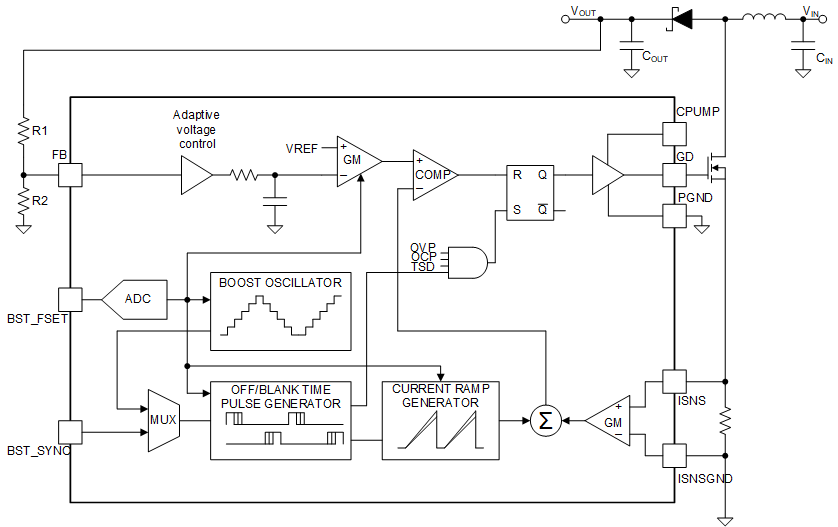
6.3.6 Boost Controller
The LP8866S-Q1 current-mode-controlled boost DC/DC controller generates the anode voltage for the LEDs. The boost is a current-mode-controlled topology with a cycle by cycle current limit. The boost converter senses the switch current and across the external sense resistor connected between ISNS and ISNSGND. A 20mΩ sense resistor results in a 10A cycle by cycle current limit. The sense resistor value could vary from 15mΩ to 50mΩ depending on the application. Maximum boost voltage is configured with external FB-pin resistor divider connected between VOUT and FB. The FB-divider equation is described in Section 6.3.6.3.
 Figure 6-3 Boost
Controller Block Diagram
Figure 6-3 Boost
Controller Block DiagramThe boost switching frequency is adjustable from 100kHz to 2.2MHz via an external resistor at BST_FSET (see Table 6-2). Resistor with 1% accuracy is needed to ensure proper operation.
| R_BST_FSET (kΩ) | BOOST FREQUENCY (kHz) |
|---|---|
| 3.92 | 400 |
| 4.75 | 200 |
| 5.76 | 303 |
| 7.87 | 100 |
| 11 | 500 |
| 17.8 | 1818 |
| 42.2 | 2000 |
| 124 | 2222 |