ZHCSLM9B August 2020 – May 2024 LP8866S-Q1
PRODUCTION DATA
- 1
- 1 特性
- 2 应用
- 3 说明
- 4 Pin Configuration and Functions
- 5 Specifications
-
6 Detailed Description
- 6.1 Overview
- 6.2 Functional Block Diagram
- 6.3
Feature Description
- 6.3.1 Control Interface
- 6.3.2 Function Setting
- 6.3.3 Device Supply (VDD)
- 6.3.4 Enable (EN)
- 6.3.5 Charge Pump
- 6.3.6 Boost Controller
- 6.3.7 LED Current Sinks
- 6.3.8 Brightness Control
- 6.3.9
Protection and Fault Detections
- 6.3.9.1 Supply Faults
- 6.3.9.2
Boost Faults
- 6.3.9.2.1 Boost Overvoltage Faults (BSTOVPL, BSTOVPH)
- 6.3.9.2.2 Boost Overcurrent Faults (BSTOCP)
- 6.3.9.2.3 LEDSET Resistor Missing Faults (LEDSET)
- 6.3.9.2.4 MODE Resistor Missing Faults (MODESEL)
- 6.3.9.2.5 FSET Resistor Missing Faults (FSET)
- 6.3.9.2.6 ISET Resistor Out of Range Faults (ISET)
- 6.3.9.2.7 Thermal Shutdown Faults (TSD)
- 6.3.9.3 LED Faults
- 6.3.9.4 Overview of the Fault and Protection Schemes
- 6.4 Device Functional Modes
- 6.5 Programming
-
7 Application and Implementation
- 7.1 Application Information
- 7.2
Typical Applications
- 7.2.1
Full Feature Application for Display Backlight
- 7.2.1.1 Design Requirements
- 7.2.1.2
Detailed Design Procedure
- 7.2.1.2.1 Inductor Selection
- 7.2.1.2.2 Output Capacitor Selection
- 7.2.1.2.3 Input Capacitor Selection
- 7.2.1.2.4 Charge Pump Output Capacitor
- 7.2.1.2.5 Charge Pump Flying Capacitor
- 7.2.1.2.6 Output Diode
- 7.2.1.2.7 Switching FET
- 7.2.1.2.8 Boost Sense Resistor
- 7.2.1.2.9 Power-Line FET
- 7.2.1.2.10 Input Current Sense Resistor
- 7.2.1.2.11 Feedback Resistor Divider
- 7.2.1.2.12 Critical Components for Design
- 7.2.1.3 Application Curves
- 7.2.2 Application with Basic/Minimal Operation
- 7.2.3
SEPIC Mode Application
- 7.2.3.1 Design Requirements
- 7.2.3.2
Detailed Design Procedure
- 7.2.3.2.1 Inductor Selection
- 7.2.3.2.2 Coupling Capacitor Selection
- 7.2.3.2.3 Output Capacitor Selection
- 7.2.3.2.4 Input Capacitor Selection
- 7.2.3.2.5 Charge Pump Output Capacitor
- 7.2.3.2.6 Charge Pump Flying Capacitor
- 7.2.3.2.7 Switching FET
- 7.2.3.2.8 Output Diode
- 7.2.3.2.9 Switching Sense Resistor
- 7.2.3.2.10 Power-Line FET
- 7.2.3.2.11 Input Current Sense Resistor
- 7.2.3.2.12 Feedback Resistor Divider
- 7.2.3.2.13 Critical Components for Design
- 7.2.3.3 Application Curves
- 7.2.1
Full Feature Application for Display Backlight
- 7.3 Power Supply Recommendations
- 7.4 Layout
- 8 Device and Documentation Support
- 9 Revision History
- 10Mechanical, Packaging, and Orderable Information
封装选项
机械数据 (封装 | 引脚)
散热焊盘机械数据 (封装 | 引脚)
订购信息
6.3.6.3 Boost Adaptive Voltage Control
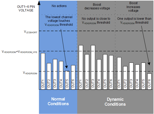
The LP8866S-Q1 boost DC/DC converter generates the anode voltage for the LEDs. During normal operation, boost output voltage is adjusted automatically based on the LED current sink headroom voltages. This is called adaptive boost control. The number of used LED outputs is set by LED_SET pin and only the active LED outputs are monitored to control the adaptive boost voltage. Any LED strings with open or short faults are also removed from the adaptive voltage control loop. The LED driver pin voltages are periodically monitored by the control loop and the boost voltage is raised if any of the LED outputs falls below the VHEADROOM threshold. The boost voltage is lowered until any of the LED outputs touch the VHEADROOM threshold. See Figure 6-4 for how the boost voltage automatically scales based on the OUTx-pin voltage, VHEADROOM and VHEADROOM_HYS.
 Figure 6-4 Adaptive
Boost Voltage Control Loop Function
Figure 6-4 Adaptive
Boost Voltage Control Loop FunctionThe resistive divider (R1, R2) defines both the minimum and maximum adaptive boost voltage levels. The feedback circuit operates the same in boost and SEPIC topologies. Choose maximum boost voltage is based on the maximum LED string voltage specification, and needs at least 1V higher than maximum LED string voltage to make current sink work normally. Before the LED drivers are active, the boost starts up to the initial boost level. The initial boost voltage is approximately in the 88% point of minimum to maximum boost voltage. Once the LED driver channels are active, the boost output voltage is adjusted automatically based on OUTx pin voltages. The FB pin resistor divider also scales the boost OVP, OCP levels and the LED short level in HUD application.