ZHCSK37 August   2019 LP8867C-Q1 , LP8869C-Q1

PRODUCTION DATA.  

  1. 特性
    1.     简化原理图
  2. 应用
  3. 说明
    1.     系统效率
  4. 修订历史记录
  5. Device Comparison Table
  6. Pin Configuration and Functions
    1.     Pin Functions
  7. Specifications
    1. 7.1  Absolute Maximum Ratings
    2. 7.2  ESD Ratings
    3. 7.3  Recommended Operating Conditions
    4. 7.4  Thermal Information
    5. 7.5  Electrical Characteristics
    6. 7.6  Internal LDO Electrical Characteristics
    7. 7.7  Protection Electrical Characteristics
    8. 7.8  Current Sinks Electrical Characteristics
    9. 7.9  PWM Brightness Control Electrical Characteristics
    10. 7.10 Boost and SEPIC Converter Characteristics
    11. 7.11 Logic Interface Characteristics
    12. 7.12 Typical Characteristics
  8. Detailed Description
    1. 8.1 Overview
    2. 8.2 Functional Block Diagram
    3. 8.3 Feature Description
      1. 8.3.1 Integrated DC-DC Converter
        1. 8.3.1.1 DC-DC Converter Parameter Configuration
          1. 8.3.1.1.1 Switching Frequency
          2. 8.3.1.1.2 Spread Spectrum and External SYNC
          3. 8.3.1.1.3 Recommended Component Value and Internal Parameters
          4. 8.3.1.1.4 DC-DC Converter Switching Current Limit
          5. 8.3.1.1.5 DC-DC Converter Light Load Mode
        2. 8.3.1.2 Adaptive Voltage Control
          1. 8.3.1.2.1 Using Two-Divider
          2. 8.3.1.2.2 Using T-Divider
          3. 8.3.1.2.3 Feedback Capacitor
      2. 8.3.2 Internal LDO
      3. 8.3.3 LED Current Sinks
        1. 8.3.3.1 LED Output Configuration
        2. 8.3.3.2 LED Current Setting
        3. 8.3.3.3 Brightness Control
      4. 8.3.4 Protection and Fault Detections
        1. 8.3.4.1 Supply Fault and Protection
          1. 8.3.4.1.1 VIN Undervoltage Fault (VIN_UVLO)
          2. 8.3.4.1.2 VIN Overvoltage Fault (VIN_OVP)
        2. 8.3.4.2 Boost Fault and Protection
          1. 8.3.4.2.1 Boost Overvoltage Fault (BST_OVP)
          2. 8.3.4.2.2 SW Overvoltage Fault (SW_OVP)
        3. 8.3.4.3 LED Fault and Protection
          1. 8.3.4.3.1 LED Open Fault (LED_OPEN)
          2. 8.3.4.3.2 LED Short Fault (LED_SHORT)
        4. 8.3.4.4 Thermal Fault and Protection (TSD)
        5. 8.3.4.5 Overview of the Fault and Protection Schemes
    4. 8.4 Device Functional Modes
      1. 8.4.1 STANDBY State
      2. 8.4.2 SOFT START State
      3. 8.4.3 BOOST START State
      4. 8.4.4 NORMAL State
      5. 8.4.5 FAULT RECOVERY State
      6. 8.4.6 State Diagram and Timing Diagram for Start-up and Shutdown
  9. Application and Implementation
    1. 9.1 Application Information
    2. 9.2 Typical Applications
      1. 9.2.1 Typical Application for 4 LED Strings
        1. 9.2.1.1 Design Requirements
        2. 9.2.1.2 Detailed Design Procedure
          1. 9.2.1.2.1 Inductor Selection
          2. 9.2.1.2.2 Output Capacitor Selection
          3. 9.2.1.2.3 Input Capacitor Selection
          4. 9.2.1.2.4 LDO Output Capacitor
          5. 9.2.1.2.5 Diode
        3. 9.2.1.3 Application Curves
      2. 9.2.2 SEPIC Mode Application
        1. 9.2.2.1 Design Requirements
        2. 9.2.2.2 Detailed Design Procedure
          1. 9.2.2.2.1 Inductor
          2. 9.2.2.2.2 Diode
          3. 9.2.2.2.3 Capacitor C1
        3. 9.2.2.3 Application Curves
  10. 10Power Supply Recommendations
  11. 11Layout
    1. 11.1 Layout Guidelines
    2. 11.2 Layout Example
  12. 12器件和文档支持
    1. 12.1 器件支持
      1. 12.1.1 开发支持
    2. 12.2 文档支持
      1. 12.2.1 相关文档
    3. 12.3 接收文档更新通知
    4. 12.4 社区资源
    5. 12.5 商标
    6. 12.6 静电放电警告
    7. 12.7 Glossary
  13. 13机械、封装和可订购信息

封装选项

机械数据 (封装 | 引脚)
散热焊盘机械数据 (封装 | 引脚)
订购信息

Adaptive Voltage Control

The LP886xC-Q1 DC/DC converter generates the supply voltage for the LEDs. During normal operation, boost output voltage is adjusted automatically based on the LED cathode (OUTx pin) voltages. This is called adaptive boost control. Only the active LED outputs are monitored to control the adaptive boost voltage. Any LED strings with open or short faults are removed from the adaptive voltage control loop. The OUTx pin voltages are periodically monitored by the control loop. The boost voltage is raised if any of the OUTx voltage falls below the VLOW_COMP threshold. The boost voltage is also lowered if all OUTx voltages are higher than VLOW_COMP threshold. The boost voltage keeps unchanged when one of OUTx voltage touches the VLOW_COMP threshold. In normal operation, the lowest voltage among the OUTx pins is around VLOW_COMP, and boost voltage stays constant. VLOW_COMP level is the minimum voltage which could guarantee proper LED current sink operation. See Figure 10 for how the boost voltage automatically scales based on the OUT1-4 pin voltage.
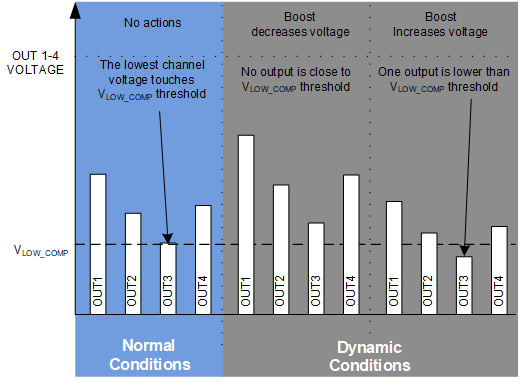
LP8867C-Q1 LP8869C-Q1 cht-01-adaptive.gifFigure 10. Adaptive Boost Voltage Control Loop Function