SNOS413E August 2000 – November 2016 LPV321-N , LPV324-N , LPV358-N
PRODUCTION DATA.
- 1 Features
- 2 Applications
- 3 Description
- 4 Revision History
- 5 Pin Configuration and Functions
- 6 Specifications
- 7 Detailed Description
- 8 Application and Implementation
- 9 Power Supply Recommendations
- 10Layout
- 11Device and Documentation Support
- 12Mechanical, Packaging, and Orderable Information
7 Detailed Description
7.1 Overview
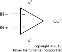
The LPV321-N, LPV358-N, and LPV324-N devices are micropower (10-µA) versions of the popular LMV3xx-N. The LPV321-N is the single-channel version. The LPV358-N is the dual, and the LPV324-N is the quad. The LPV32x-N are the most cost effective solution for applications where low power and low voltage operation, space efficiency, and low-price are important. The LPV3x-N have rail-to-rail output swing capability and the input common-mode voltage range includes ground. They all exhibit excellent speed to power ratio, achieving 152 kHz of bandwidth and 0.1-V/µs slew rate with 10 mA of supply current.
7.2 Functional Block Diagram
7.3 Feature Description
7.3.1 Size
The small footprints of the LPV3xx-N packages save space on printed circuit boards, and enable the design of smaller electronic products (such as cellular phones, pagers, or other portable systems). The low profile of the LPV3xx-N make them possible to use in PCMCIA type III cards.
7.3.2 Signal Integrity
Signals can pick up noise between the signal source and the amplifier. By using a physically smaller amplifier package, the LPV3xx-N can be placed closer to the signal source, reducing noise pickup and increasing signal integrity.
7.3.3 Simplified Board Layout
These products help avoid using long printed-circuit traces in the PCB. This means no additional components, such as capacitors and resistors, are needed to filter out unwanted signals due to the interference between the long printed-circuit traces.
7.3.4 Low Supply Current
These devices help maximize battery life. They are ideal for battery powered systems.
7.3.5 Low Supply Voltage
TI provides ensured performance at 2.7 V and 5 V. These specifications ensure operation throughout the battery lifetime.
7.3.6 Rail-to-Rail Output
Rail-to-rail output swing provides maximum possible dynamic range at the output. This is particularly important when operating on low-supply voltages.
7.3.7 Input Includes Ground
Allows direct sensing near GND in single supply operation.
The differential input voltage may be larger than V+ without damaging the device. Protection should be provided to prevent the input voltages from going negative more than −0.3 V (at 25°C). An input clamp diode with a resistor to the IC input terminal can be used.
7.4 Device Functional Modes
The LPV3xx-N can be operated as a single-supply or a dual-supply operational amplifier depending on the application.
7.4.1 Capacitive Load Tolerance
The LPV3xx-N can directly drive 200 pF in unity-gain without oscillation. The unity-gain follower is the most sensitive configuration to capacitive loading. Direct capacitive loading reduces the phase margin of amplifiers. The combination of the amplifier's output impedance and the capacitive load induces phase lag. This results in either an underdamped pulse response or oscillation. To drive a heavier capacitive load, circuit in Figure 37 can be used.
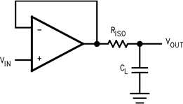 Figure 37. Indirectly Driving A Capacitive Load Using Resistive Isolation
In Figure 37, the isolation resistor (RISO) and the load capacitor (CL) form a pole to increase stability by adding more phase margin to the overall system. The desired performance depends on the value of RISO. The bigger the RISO resistor value, the more stable VOUT is. Figure 38 is an output waveform of Figure 37 using 100 kΩ for RISO and 1000 pF for CL.
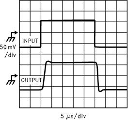 Figure 38. Pulse Response of the LPV324 Circuit in Figure 37
The circuit in Figure 39 is an improvement to the one in Figure 37 because it provides DC accuracy as well as AC stability. If there were a load resistor in Figure 37, the output would be voltage divided by RISO and the load resistor. Instead, in Figure 39, RF provides the DC accuracy by using feed-forward techniques to connect VIN to RL. Caution is needed in choosing the value of RF due to the input bias current of the LPV3xx-N. CF and RISO serve to counteract the loss of phase margin by feeding the high frequency component of the output signal back to the amplifier's inverting input, thereby preserving phase margin in the overall feedback loop. Increased capacitive drive is possible by increasing the value of CF. This in turn slows down the pulse response.
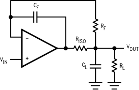 Figure 39. Indirectly Driving A Capacitive Load With DC Accuracy
7.4.2 Input Bias Current Cancellation
The LPV3xx-N family has a bipolar input stage. The typical input bias current of LPV3xx-N is 1.5 nA with 5-V supply. Thus a 100-kΩ input resistor causes 0.15 mV of error voltage. By balancing the resistor values at both inverting and noninverting inputs, the error caused by the amplifier's input bias current is reduced. The circuit in Figure 40 shows how to cancel the error caused by input bias current.
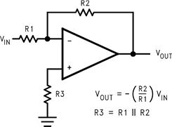 Figure 40. Cancelling the Error Caused by Input Bias Current