ZHCSD68H July 2014 – April 2021 LSF0204 , LSF0204D
PRODUCTION DATA
- 1 特性
- 2 应用
- 3 说明
- 4 Revision History
- 5 说明(续)
- 6 Pin Configuration and Functions
-
7 Specifications
- 7.1 Absolute Maximum Ratings
- 7.2 ESD Ratings
- 7.3 Recommended Operating Conditions
- 7.4 Thermal Information
- 7.5 Electrical Characteristics
- 7.6 Switching Characteristics: AC Performance (Translating Down, 3.3 V to 1.8 V)
- 7.7 Switching Characteristics: AC Performance (Translating Down, 3.3 V to 1.2 V)
- 7.8 Switching Characteristics: AC Performance (Translating Up, 1.8 V to 3.3 V)
- 7.9 Switching Characteristics: AC Performance (Translating Up, 1.2 V to 1.8 V)
- 7.10 Typical Characteristics
- 8 Parameter Measurement Information
- 9 Detailed Description
- 10Application and Implementation
- 11Power Supply Recommendations
- 12Layout
- 13Device and Documentation Support
- 14Mechanical, Packaging, and Orderable Information
封装选项
请参考 PDF 数据表获取器件具体的封装图。
机械数据 (封装 | 引脚)
- RGY|14
- YZP|12
- RUT|12
- PW|14
散热焊盘机械数据 (封装 | 引脚)
- RGY|14
订购信息
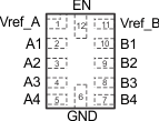
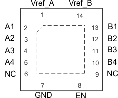
6 Pin Configuration and Functions
 Figure 6-1 PW Package,
14-Pin TSSOP
(Top View)
 Figure 6-3 RUT Package,
12-Pin UQFN
(Transparent Top View)
 Figure 6-2 RGY Package,
14-Pin VQFN
(Transparent Top View)
 Figure 6-4 YZP Package,
12-Pin DSBGA
(Transparent Top View)
Table 6-1 Pin Functions
| PIN | TYPE(1) | DESCRIPTION | ||||
|---|---|---|---|---|---|---|
| NAME | NO. | |||||
| PW, RGY | RUT | YZP | ||||
| Vref_A | 1 | 1 | B2 | — | Reference supply voltage; see Application and Implementation section | |
| A1 | 2 | 2 | A3 | I/O | Input/output 1. | |
| A2 | 3 | 3 | B3 | I/O | Input/output 2. | |
| A3 | 4 | 4 | C3 | I/O | Input/output 3. | |
| A4 | 5 | 5 | D3 | I/O | Input/output 4. | |
| NC | 6 | – | — | — | No connection. Not internally connected. | |
| GND | 7 | 6 | D2 | — | Ground | |
| EN | 8 | 12 | C2 | I | Switch enable input; LSF0204: EN is high-active; LSF0204D: EN is low-active | |
| NC | 9 | – | — | — | No connection. Not internally connected. | |
| B4 | 10 | 7 | D1 | I/O | Input/output 4. | |
| B3 | 11 | 8 | C1 | I/O | Input/output 3. | |
| B2 | 12 | 9 | B1 | I/O | Input/output 2. | |
| B1 | 13 | 10 | A1 | I/O | Input/output 1. | |
| Vref_B | 14 | 11 | A2 | — | Reference supply voltage; see Application and Implementation section | |
(1) I = input, O = output