SLOS018I May 1988 – July 2016 LT1013 , LT1013AM , LT1013D , LT1013M
PRODUCTION DATA.
- 1 Features
- 2 Applications
- 3 Description
- 4 Revision History
- 5 Pin Configuration and Functions
-
6 Specifications
- 6.1 Absolute Maximum Ratings
- 6.2 ESD Ratings
- 6.3 Recommended Operating Conditions
- 6.4 Thermal Information
- 6.5 Electrical Characteristics: LT1013C, ±15 V
- 6.6 Electrical Characteristics: LT1013C, 5 V
- 6.7 Electrical Characteristics: LT1013D, ±15 V
- 6.8 Electrical Characteristics: LT1013D, 5 V
- 6.9 Electrical Characteristics: LT1013DI, ±15 V
- 6.10 Electrical Characteristics: LT1013DI, 5 V
- 6.11 Electrical Characteristics: LT1013M, ±15 V
- 6.12 Electrical Characteristics: LT1013M, 5 V
- 6.13 Electrical Characteristics: LT1013AM, ±15 V
- 6.14 Electrical Characteristics: LT1013AM, 5 V
- 6.15 Electrical Characteristics: LT1013DM, ±15 V
- 6.16 Electrical Characteristics: LT1013DM, 5 V
- 6.17 Operating Characteristics
- 6.18 Typical Characteristics
- 7 Detailed Description
- 8 Application and Implementation
- 9 Power Supply Recommendations
- 10Layout
- 11Device and Documentation Support
- 12Mechanical, Packaging, and Orderable Information
7 Detailed Description
7.1 Overview
The LT1013x device is a dual operational amplifier with low natural VIO without programming memory that can be erased. There are no side effects from active VIO correction used by other op amps. The LT1013x has built-in protection for input voltage below VCC–. However, an external resistance must be add to protect the LT1013x from input voltage greater than VCC+.
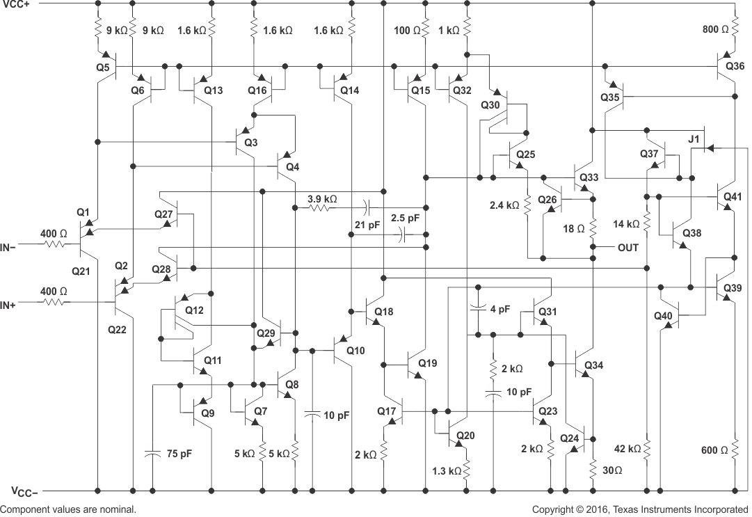
7.2 Functional Block Diagram

7.3 Feature Description
7.3.1 Input Resistors
For voltages less than VCC–, a pair of 400-Ω resistors limit input current. These resistors have parasitic diodes to VCC+. Therefore, external series resistance is needed if input voltage exceed VCC+
7.3.2 Output Stage
High output is provided by Q33 emitter for low output impedance. Q26 provides active current limiting for sourcing current.
Low output is provided by Q34 collector for lower output voltage near VCC– rail. Q24 provides active current limiting for sinking current.
7.3.3 Low-Supply Operation
The minimum supply voltage for proper operation of the LT1013x is 3.4 V (three NiCad batteries). Typical supply current at this voltage is 290 µA; therefore, power dissipation is only 1 mW per amplifier.
7.3.4 Output Phase Reversal Protection
The LT1013x is fully specified for single-supply operation (VCC− = 0). The common-mode input voltage range includes ground, and the output swings to within a few millivolts of ground.
Furthermore, the LT1013x has specific circuitry that addresses the difficulties of single-supply operation, both at the input and at the output. At the input, the driving signal can fall below 0 V, either inadvertently or on a transient basis. If the input is more than a few hundred millivolts below ground, the LT1013x is designed to deal with the following two problems that can occur:
- On many other operational amplifiers, when the input is more than a diode drop below ground, unlimited current flows from the substrate (VCC− terminal) to the input, which can destroy the unit. On the LT1013x, the 400-Ω resistors in series with the input protect the device, even when the input is 5 V below ground.
- When the input is more than 400 mV below ground (at TA = 25°C), the input stage of similar operational amplifiers saturates, and phase reversal occurs at the output. This can cause lockup in servo systems. Because of unique phase-reversal protection circuitry (Q21, Q22, Q27, and Q28), the LT1013x outputs do not reverse, even when the inputs are at −1.5 V (see Figure 24).
This phase-reversal protection circuitry does not function when the other operational amplifier on the LT1013x is driven hard into negative saturation at the output. Phase-reversal protection does not work on amplifier 1 when amplifier 2 output is in negative saturation nor on amplifier 2 when amplifier 1 output is in negative saturation.
At the output, other single-supply designs either cannot swing to within 600 mV of ground or cannot sink more than a few micro amperes while swinging to ground. The all-npn output stage of the LT1013x maintains its low output resistance and high-gain characteristics until the output is saturated. In dual-supply operations, the output stage is free of crossover distortion.
 Figure 24. Voltage-Follower Response With Input Exceeding the Negative Common-Mode Input Voltage Range
7.3.4.1 Comparator Applications
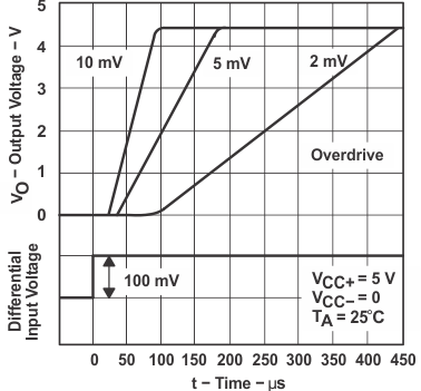
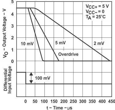
The single-supply operation of the LT1013x is well suited for use as a precision comparator with TTL-compatible output. In systems using both operational amplifiers and comparators, the LT1013x can perform multiple duties (see Figure 25 and Figure 26).
 Figure 25. Low-to-High-Level Output Response for Various Input Overdrives
 Figure 26. High-to-Low-Level Output Response for Various Input Overdrives
7.4 Device Functional Modes
The LT1013x dual operational amplifier amplifies a differential voltage applied to the inputs.