ZHCSRT4 august   2023 LV5144

PRODUCTION DATA  

  1.   1
  2. 特性
  3. 应用
  4. 说明
  5. Revision History
  6. 说明(续)
  7. Pin Configuration and Functions
    1. 6.1 Wettable Flanks
  8. Specifications
    1. 7.1 Absolute Maximum Ratings
    2. 7.2 ESD Ratings
    3. 7.3 Recommended Operating Conditions
    4. 7.4 Thermal Information
    5. 7.5 Electrical Characteristics
    6. 7.6 Typical Characteristics
  9. Detailed Description
    1. 8.1 Overview
    2. 8.2 Functional Block Diagram
    3. 8.3 Feature Description
      1. 8.3.1  Input Range (VIN)
      2. 8.3.2  Output Voltage Setpoint and Accuracy (FB)
      3. 8.3.3  High-Voltage Bias Supply Regulator (VCC)
      4. 8.3.4  Precision Enable (EN/UVLO)
      5. 8.3.5  Power Good Monitor (PGOOD)
      6. 8.3.6  Switching Frequency (RT, SYNCIN)
        1. 8.3.6.1 Frequency Adjust
        2. 8.3.6.2 Clock Synchronization
      7. 8.3.7  Configurable Soft Start (SS/TRK)
        1. 8.3.7.1 Tracking
      8. 8.3.8  Voltage-Mode Control (COMP)
      9. 8.3.9  Gate Drivers (LO, HO)
      10. 8.3.10 Current Sensing and Overcurrent Protection (ILIM)
      11. 8.3.11 OCP Duty Cycle Limiter
    4. 8.4 Device Functional Modes
      1. 8.4.1 Shutdown Mode
      2. 8.4.2 Standby Mode
      3. 8.4.3 Active Mode
      4. 8.4.4 Diode Emulation Mode
      5. 8.4.5 Thermal Shutdown
  10. Application and Implementation
    1. 9.1 Application Information
      1. 9.1.1 Design and Implementation
      2. 9.1.2 Power Train Components
        1. 9.1.2.1 Inductor
        2. 9.1.2.2 Output Capacitors
        3. 9.1.2.3 Input Capacitors
        4. 9.1.2.4 Power MOSFETs
      3. 9.1.3 Control Loop Compensation
      4. 9.1.4 EMI Filter Design
    2. 9.2 Typical Applications
      1. 9.2.1 Design 1 – 12-A High-Efficiency Synchronous Buck DC/DC Regulator
        1. 9.2.1.1 Design Requirements
        2. 9.2.1.2 Detailed Design Procedure
        3. 9.2.1.3 Application Curves
      2. 9.2.2 Design 2 – High Density, 12-V, 8-A Rail From 48-V Telecom Power
        1. 9.2.2.1 Design Requirements
        2. 9.2.2.2 Detailed Design Procedure
        3. 9.2.2.3 Application Curves
    3. 9.3 Power Supply Recommendations
    4. 9.4 Layout
      1. 9.4.1 Layout Guidelines
        1. 9.4.1.1 Power Stage Layout
        2. 9.4.1.2 Gate Drive Layout
        3. 9.4.1.3 PWM Controller Layout
        4. 9.4.1.4 Thermal Design and Layout
        5. 9.4.1.5 Ground Plane Design
      2. 9.4.2 Layout Example
  11. 10Device and Documentation Support
    1. 10.1 Device Support
      1. 10.1.1 第三方米6体育平台手机版_好二三四免责声明
      2. 10.1.2 Development Support
    2. 10.2 Documentation Support
      1. 10.2.1 Related Documentation
        1. 10.2.1.1 PCB Layout Resources
        2. 10.2.1.2 Thermal Design Resources
    3. 10.3 接收文档更新通知
    4. 10.4 支持资源
    5. 10.5 Trademarks
    6. 10.6 静电放电警告
    7. 10.7 术语表
  12. 11Mechanical, Packaging, and Orderable Information

封装选项

机械数据 (封装 | 引脚)
散热焊盘机械数据 (封装 | 引脚)
订购信息

Layout Example

Figure 9-34 shows an example PCB layout based on the LV5144-Q1-EVM12V design. The power component connections are made on the top layer with wide, copper-filled polygon areas. The SW connection from the power MOSFETs to the inductor is purposely kept at minimum area to reduce radiated EMI. A power ground plane is placed on layer 2 with 6 mil (0.15 mm) spacing to the top layer, see Figure 9-35. As a result, the buck regulator hot loop has a small effective area based on this tightly-coupled GND plane directly underneath the MOSFETs.

The LV5144 controller is located close to the gate terminals of the MOSFETs such that the gate drive traces are routed short and direct. Refer to the LV5144-Q1-EVM12V Evaluation Module User's Guide for more detail.
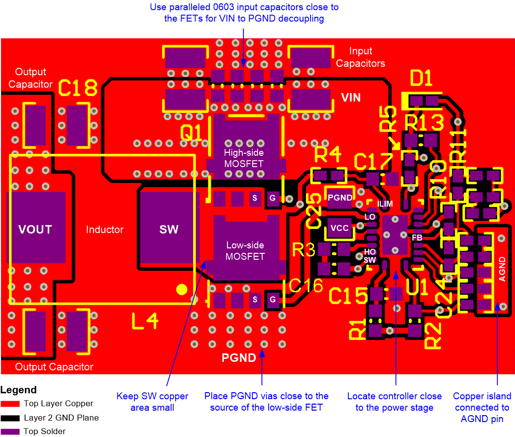
GUID-7ACABD31-40DA-4EA1-AB7C-46DD248B400D-low.gif Figure 9-34 LV5144 Controller PCB Layout (Viewed From Top)
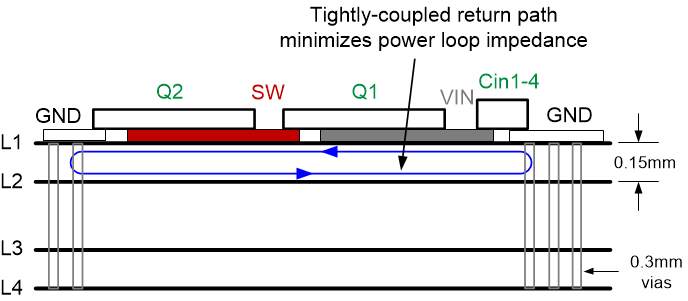
GUID-FF32B7DD-403F-414A-8B77-289280EA047D-low.gif Figure 9-35 PCB Stack-up Diagram With Low L1-L2 Intra-layer Spacing