ZHCSOU8B August   2021  – February 2022 MCT8316A

PRODUCTION DATA  

  1. 特性
  2. 应用
  3. 说明
  4. Revision History
  5. Device Comparison Table
  6. Pin Configuration and Functions
  7. Specifications
    1. 7.1 Absolute Maximum Ratings
    2. 7.2 ESD Ratings
    3. 7.3 Recommended Operating Conditions
    4. 7.4 Thermal Information
    5. 7.5 Electrical Characteristics
    6. 7.6 Characteristics of the SDA and SCL bus for Standard and Fast mode
    7. 7.7 Typical Characteristics
  8. Detailed Description
    1. 8.1 Overview
    2. 8.2 Functional Block Diagram
    3. 8.3 Feature Description
      1. 8.3.1  Output Stage
      2. 8.3.2  Device Interface Modes
        1. 8.3.2.1 Interface - Control and Monitoring
        2. 8.3.2.2 I2C Interface
        3. 8.3.2.3 Hardware Interface - Pin Configuration
      3. 8.3.3  Step-Down Mixed-Mode Buck Regulator
        1. 8.3.3.1 Buck in Inductor Mode
        2. 8.3.3.2 Buck in Resistor mode
        3. 8.3.3.3 Buck Regulator with External LDO
        4. 8.3.3.4 AVDD Power Sequencing from Buck Regulator
        5. 8.3.3.5 Mixed Mode Buck Operation and Control
        6. 8.3.3.6 Buck Undervoltage Protection
        7. 8.3.3.7 Buck Overcurrent Protection
      4. 8.3.4  AVDD Linear Voltage Regulator
      5. 8.3.5  Charge Pump
      6. 8.3.6  Slew Rate Control
      7. 8.3.7  Cross Conduction (Dead Time)
      8. 8.3.8  SPEED Control
        1. 8.3.8.1 Analog-Mode Speed Control
        2. 8.3.8.2 PWM-Mode Speed Control
        3. 8.3.8.3 I2C based Speed Control
        4. 8.3.8.4 Frequency-Mode Speed Control
      9. 8.3.9  Starting the Motor Under Different Initial Conditions
        1. 8.3.9.1 Case 1 – Motor is Stationary
        2. 8.3.9.2 Case 2 – Motor is Spinning in the Forward Direction
        3. 8.3.9.3 Case 3 – Motor is Spinning in the Reverse Direction
      10. 8.3.10 Motor Start Sequence (MSS)
        1. 8.3.10.1 Initial Speed Detect (ISD)
        2. 8.3.10.2 Motor Resynchronization
        3. 8.3.10.3 Reverse Drive
        4. 8.3.10.4 Motor Start-up
          1. 8.3.10.4.1 Align
          2. 8.3.10.4.2 Double Align
          3. 8.3.10.4.3 Initial Position Detection (IPD)
            1. 8.3.10.4.3.1 IPD Operation
            2. 8.3.10.4.3.2 IPD Release Mode
            3. 8.3.10.4.3.3 IPD Advance Angle
          4. 8.3.10.4.4 Slow First Cycle Startup
          5. 8.3.10.4.5 Open loop
          6. 8.3.10.4.6 Transition from Open to Closed Loop
      11. 8.3.11 Closed Loop Operation
        1. 8.3.11.1 120o Commutation
          1. 8.3.11.1.1 High-Side Modulation
          2. 8.3.11.1.2 Low-Side Modulation
          3. 8.3.11.1.3 Mixed Modulation
        2. 8.3.11.2 Variable Commutation (Available only in MCT8316AV)
        3. 8.3.11.3 Lead Angle Control
        4. 8.3.11.4 Closed loop accelerate
      12. 8.3.12 Speed Loop (Available only in MCT8316AV)
      13. 8.3.13 Input Power Regulation (Available only in MCT8316AV)
      14. 8.3.14 Anti-Voltage Surge (AVS)
      15. 8.3.15 Output PWM Switching Frequency
      16. 8.3.16 Fast Start-up (< 50 ms)
        1. 8.3.16.1 BEMF Threshold
        2. 8.3.16.2 Dynamic Degauss
      17. 8.3.17 Fast Deceleration
      18. 8.3.18 Active Demagnetization
        1. 8.3.18.1 Active Demagnetization in action
      19. 8.3.19 Motor Stop Options
        1. 8.3.19.1 Coast (Hi-Z) Mode
        2. 8.3.19.2 Recirculation Mode
        3. 8.3.19.3 Low-Side Braking
        4. 8.3.19.4 High-Side Braking
        5. 8.3.19.5 Active Spin-Down
      20. 8.3.20 FG Configuration
        1. 8.3.20.1 FG Output Frequency
        2. 8.3.20.2 FG Open-Loop and Lock Behavior
      21. 8.3.21 Protections
        1. 8.3.21.1  VM Supply Undervoltage Lockout
        2. 8.3.21.2  AVDD Undervoltage Lockout (AVDD_UV)
        3. 8.3.21.3  BUCK Undervoltage Lockout (BUCK_UV)
        4. 8.3.21.4  VCP Charge Pump Undervoltage Lockout (CPUV)
        5. 8.3.21.5  Overvoltage Protection (OVP)
        6. 8.3.21.6  Overcurrent Protection (OCP)
          1. 8.3.21.6.1 OCP Latched Shutdown (OCP_MODE = 00b)
          2. 8.3.21.6.2 OCP Automatic Retry (OCP_MODE = 01b)
          3. 8.3.21.6.3 OCP Report Only (OCP_MODE = 10b)
          4. 8.3.21.6.4 OCP Disabled (OCP_MODE = 11b)
        7. 8.3.21.7  Buck Overcurrent Protection
        8. 8.3.21.8  Cycle-by-Cycle (CBC) Current Limit (CBC_ILIMIT)
          1. 8.3.21.8.1 CBC_ILIMIT Automatic Recovery next PWM Cycle (CBC_ILIMIT_MODE = 000xb)
          2. 8.3.21.8.2 CBC_ILIMIT Automatic Recovery Threshold Based (CBC_ILIMIT_MODE = 001xb)
          3. 8.3.21.8.3 CBC_ILIMIT Automatic Recovery after 'n' PWM Cycles (CBC_ILIMIT_MODE = 010xb)
          4. 8.3.21.8.4 CBC_ILIMIT Report Only (CBC_ILIMIT_MODE = 0110b)
          5. 8.3.21.8.5 CBC_ILIMIT Disabled (CBC_ILIMIT_MODE = 0111b or 1xxxb)
        9. 8.3.21.9  Lock Detection Current Limit (LOCK_ILIMIT)
          1. 8.3.21.9.1 LOCK_ILIMIT Latched Shutdown (LOCK_ILIMIT_MODE = 00xxb)
          2. 8.3.21.9.2 LOCK_ILIMIT Automatic Recovery (LOCK_ILIMIT_MODE = 01xxb)
          3. 8.3.21.9.3 LOCK_ILIMIT Report Only (LOCK_ILIMIT_MODE = 1000b)
          4. 8.3.21.9.4 LOCK_ILIMIT Disabled (LOCK_ILIMIT_MODE = 1xx1b)
        10. 8.3.21.10 Thermal Warning (OTW)
        11. 8.3.21.11 Thermal Shutdown (TSD)
        12. 8.3.21.12 Motor Lock (MTR_LCK)
          1. 8.3.21.12.1 MTR_LCK Latched Shutdown (MTR_LCK_MODE = 00xxb)
          2. 8.3.21.12.2 MTR_LCK Automatic Recovery (MTR_LCK_MODE= 01xxb)
          3. 8.3.21.12.3 MTR_LCK Report Only (MTR_LCK_MODE = 1000b)
          4. 8.3.21.12.4 MTR_LCK Disabled (MTR_LCK_MODE = 1xx1b)
        13. 8.3.21.13 Motor Lock Detection
          1. 8.3.21.13.1 Lock 1: Abnormal Speed (ABN_SPEED)
          2. 8.3.21.13.2 Lock 2: Loss of Sync (LOSS_OF_SYNC)
          3. 8.3.21.13.3 Lock3: No-Motor Fault (NO_MTR)
        14. 8.3.21.14 IPD Faults
    4. 8.4 Device Functional Modes
      1. 8.4.1 Functional Modes
        1. 8.4.1.1 Sleep Mode
        2. 8.4.1.2 Standby Mode
        3. 8.4.1.3 Fault Reset (CLR_FLT)
    5. 8.5 External Interface
      1. 8.5.1 DRVOFF Functionality
      2. 8.5.2 DAC outputs
      3. 8.5.3 SOX Output
      4. 8.5.4 Oscillator Source
        1. 8.5.4.1 External Clock Source (Available for MCT8316AV)
      5. 8.5.5 External Watchdog (Available only in MCT836AV)
    6. 8.6 EEPROM access and I2C interface
      1. 8.6.1 EEPROM Access
        1. 8.6.1.1 EEPROM Write
        2. 8.6.1.2 EEPROM Read
      2. 8.6.2 I2C Serial Interface (Available only in MCT8316AV)
        1. 8.6.2.1 I2C Data Word
        2. 8.6.2.2 I2C Write Operation
        3. 8.6.2.3 I2C Read Operation
        4. 8.6.2.4 Examples of MCT8316A I2C Communication Protocol Packets
        5. 8.6.2.5 Internal Buffers
        6. 8.6.2.6 CRC Byte Calculation
    7. 8.7 EEPROM (Non-Volatile) Register Map
      1. 8.7.1 Algorithm_Configuration Registers
      2. 8.7.2 Fault_Configuration Registers
      3. 8.7.3 Hardware_Configuration Registers
      4. 8.7.4 Gate_Driver_Configuration Registers
    8. 8.8 RAM (Volatile) Register Map
      1. 8.8.1 Fault_Status Registers
      2. 8.8.2 System_Status Registers
      3. 8.8.3 Algo_Control Registers
      4. 8.8.4 Device_Control Registers
  9. Application and Implementation
    1. 9.1 Application Information
    2. 9.2 Typical Applications
      1. 9.2.1 Application curves
        1. 9.2.1.1 Motor startup
        2. 9.2.1.2 120o and variable commutation
        3. 9.2.1.3 Faster startup time
        4. 9.2.1.4 Setting the BEMF threshold
        5. 9.2.1.5 Maximum speed
        6. 9.2.1.6 Faster deceleration
  10. 10Power Supply Recommendations
    1. 10.1 Bulk Capacitance
  11. 11Layout
    1. 11.1 Layout Guidelines
    2. 11.2 Layout Example
    3. 11.3 Thermal Considerations
      1. 11.3.1 Power Dissipation
  12. 12Device and Documentation Support
    1. 12.1 支持资源
    2. 12.2 Trademarks
    3. 12.3 Electrostatic Discharge Caution
    4. 12.4 术语表
  13. 13Mechanical, Packaging, and Orderable Information
    1. 13.1 Tape and Reel Information

封装选项

机械数据 (封装 | 引脚)
散热焊盘机械数据 (封装 | 引脚)
订购信息
Low-Side Modulation

Low-side modulation can be configured by setting PWM_MODUL to 01b. In low-side modulation, for a given commutation state, one of the low-side FETs is switching with the commanded duty cycle DUTY_OUT, while the high-side FET is ON with 100% duty cycle (see Figure 8-27).
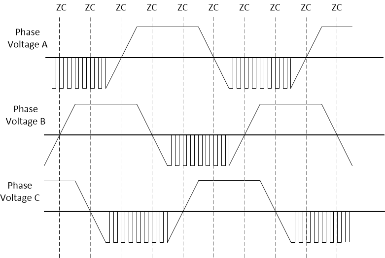
GUID-28DB9CE0-F49E-4EF5-A2D4-CD8D6640935F-low.gifFigure 8-27 120 o commutation in Low Side Modulation Mode