ZHCSNP1A March   2021  – October 2021 MCT8316Z

PRODUCTION DATA  

  1. 特性
  2. 应用
  3. 说明
  4. Revision History
  5. Device Comparison Table
  6. Pin Configuration and Functions
    1.     Pin Functions
  7. Specifications
    1. 7.1 Absolute Maximum Ratings
    2. 7.2 ESD Ratings
    3. 7.3 Recommended Operating Conditions
    4. 7.4 Thermal Information
    5. 7.5 Electrical Characteristics
    6. 7.6 SPI Timing Requirements
    7. 7.7 SPI Secondary Mode Timings
    8. 7.8 Typical Characteristics
  8. Detailed Description
    1. 8.1 Overview
    2. 8.2 Functional Block Diagram
    3. 8.3 Feature Description
      1. 8.3.1  Output Stage
      2. 8.3.2  PWM Control Mode (1x PWM Mode)
        1. 8.3.2.1 Analog Hall Input Configuration
        2. 8.3.2.2 Digital Hall Input Configuration
        3. 8.3.2.3 Asynchronous Modulation
        4. 8.3.2.4 Synchronous Modulation
        5. 8.3.2.5 Motor Operation
      3. 8.3.3  Device Interface Modes
        1. 8.3.3.1 Serial Peripheral Interface (SPI)
        2. 8.3.3.2 Hardware Interface
      4. 8.3.4  Step-Down Mixed-Mode Buck Regulator
        1. 8.3.4.1 Buck in Inductor Mode
        2. 8.3.4.2 Buck in Resistor mode
        3. 8.3.4.3 Buck Regulator with External LDO
        4. 8.3.4.4 AVDD Power Sequencing on Buck Regulator
        5. 8.3.4.5 Mixed mode Buck Operation and Control
      5. 8.3.5  AVDD Linear Voltage Regulator
      6. 8.3.6  Charge Pump
      7. 8.3.7  Slew Rate Control
      8. 8.3.8  Cross Conduction (Dead Time)
      9. 8.3.9  Propagation Delay
        1. 8.3.9.1 Driver Delay Compensation
      10. 8.3.10 Pin Diagrams
        1. 8.3.10.1 Logic Level Input Pin (Internal Pulldown)
        2. 8.3.10.2 Logic Level Input Pin (Internal Pullup)
        3. 8.3.10.3 Open Drain Pin
        4. 8.3.10.4 Push Pull Pin
        5. 8.3.10.5 Four Level Input Pin
        6. 8.3.10.6 Seven Level Input Pin
      11. 8.3.11 Active Demagnetization
        1. 8.3.11.1 Automatic Synchronous Rectification Mode (ASR Mode)
          1. 8.3.11.1.1 Automatic Synchronous Rectification in Commutation
          2. 8.3.11.1.2 Automatic Synchronous Rectification in PWM Mode
        2. 8.3.11.2 Automatic Asynchronous Rectification Mode (AAR Mode)
      12. 8.3.12 Cycle-by-Cycle Current Limit
        1. 8.3.12.1 Cycle by Cycle Current Limit with 100% Duty Cycle Input
      13. 8.3.13 Hall Comparators (Analog Hall Inputs)
      14. 8.3.14 Advance Angle
      15. 8.3.15 FGOUT Signal
      16. 8.3.16 Protections
        1. 8.3.16.1  VM Supply Undervoltage Lockout (NPOR)
        2. 8.3.16.2  AVDD Undervoltage Lockout (AVDD_UV)
        3. 8.3.16.3  BUCK Undervoltage Lockout (BUCK_UV)
        4. 8.3.16.4  VCP Charge Pump Undervoltage Lockout (CPUV)
        5. 8.3.16.5  Overvoltage Protections (OV)
        6. 8.3.16.6  Overcurrent Protection (OCP)
          1. 8.3.16.6.1 OCP Latched Shutdown (OCP_MODE = 00b)
          2. 8.3.16.6.2 OCP Automatic Retry (OCP_MODE = 01b)
          3. 8.3.16.6.3 OCP Report Only (OCP_MODE = 10b)
          4. 8.3.16.6.4 OCP Disabled (OCP_MODE = 11b)
        7. 8.3.16.7  Buck Overcurrent Protection
        8. 8.3.16.8  Motor Lock (MTR_LOCK)
          1. 8.3.16.8.1 MTR_LOCK Latched Shutdown (MTR_LOCK_MODE = 00b)
          2. 8.3.16.8.2 MTR_LOCK Automatic Retry (MTR_LOCK_MODE = 01b)
          3. 8.3.16.8.3 MTR_LOCK Report Only (MTR_LOCK_MODE= 10b)
          4. 8.3.16.8.4 MTR_LOCK Disabled (MTR_LOCK_MODE = 11b)
          5. 8.3.16.8.5 77
        9. 8.3.16.9  Thermal Warning (OTW)
        10. 8.3.16.10 Thermal Shutdown (OTS)
    4. 8.4 Device Functional Modes
      1. 8.4.1 Functional Modes
        1. 8.4.1.1 Sleep Mode
        2. 8.4.1.2 Operating Mode
        3. 8.4.1.3 Fault Reset (CLR_FLT or nSLEEP Reset Pulse)
      2. 8.4.2 DRVOFF functionality
    5. 8.5 SPI Communication
      1. 8.5.1 Programming
        1. 8.5.1.1 SPI Format
    6. 8.6 Register Map
      1. 8.6.1 STATUS Registers
      2. 8.6.2 CONTROL Registers
  9. Application and Implementation
    1. 9.1 Application Information
    2. 9.2 Hall Sensor Configuration and Connection
      1. 9.2.1 Typical Configuration
      2. 9.2.2 Open Drain Configuration
      3. 9.2.3 Series Configuration
      4. 9.2.4 Parallel Configuration
    3. 9.3 Typical Applications
      1. 9.3.1 Three-Phase Brushless-DC Motor Control With Current Limit
        1. 9.3.1.1 Detailed Design Procedure
          1. 9.3.1.1.1 Motor Voltage
          2. 9.3.1.1.2 Using Active Demagnetization
          3. 9.3.1.1.3 Using Delay Compensation
          4. 9.3.1.1.4 Using the Buck Regulator
          5. 9.3.1.1.5 Power Dissipation and Junction Temperature Losses
        2. 9.3.1.2 Application Curves
  10. 10Power Supply Recommendations
    1. 10.1 Bulk Capacitance
  11. 11Layout
    1. 11.1 Layout Guidelines
    2. 11.2 Layout Example
    3. 11.3 Thermal Considerations
      1. 11.3.1 Power Dissipation
  12. 12Device and Documentation Support
    1. 12.1 支持资源
    2. 12.2 Trademarks
    3. 12.3 Electrostatic Discharge Caution
    4. 12.4 术语表

封装选项

机械数据 (封装 | 引脚)
散热焊盘机械数据 (封装 | 引脚)
订购信息

Hall Comparators (Analog Hall Inputs)

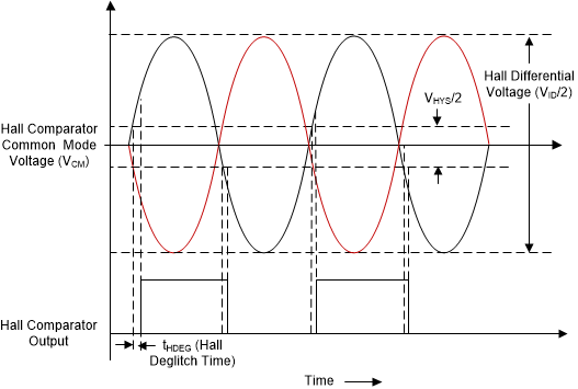
Three comparators are provided to process the raw signals from the Hall-effect sensors to commutate the motor. The Hall comparators sense the zero crossings of the differential inputs and pass the information to digital logic. The Hall comparators have hysteresis, and their detect threshold is centered at 0. The hysteresis is defined as shown in Figure 8-39.

In addition to the hysteresis, the Hall inputs are deglitched with a circuit that ignores any extra Hall transitions for a period of tHDEG after sensing a valid transition. Ignoring these transitions for the tHDEG time prevents PWM noise from being coupled into the Hall inputs, which can result in erroneous commutation.

If excessive noise is still coupled into the Hall comparator inputs, adding capacitors between the positive and negative inputs of the Hall comparators may be required. The ESD protection circuitry on the Hall inputs implements a diode to the AVDD pin. Because of this diode, the voltage on the Hall inputs should not exceed the AVDD voltage.

Because the AVDD pin is disabled in sleep mode (nSLEEP inactive), the Hall inputs should not be driven by external voltages in sleep mode. If the Hall sensors are powered externally, the supply to the Hall sensors should be disabled if the MCT8316Z device is put into sleep mode. In addition, the Hall sensors' power supply should be powered up after enabling the motor otherwise an invalid Hall state may cause a delay in motor operation.
GUID-1E0F6175-0B04-4B7B-8CD4-38F3D352C610-low.gifFigure 8-39 Hall Comparators Operation