ZHCSNP1A March 2021 – October 2021 MCT8316Z
PRODUCTION DATA
- 1 特性
- 2 应用
- 3 说明
- 4 Revision History
- 5 Device Comparison Table
- 6 Pin Configuration and Functions
- 7 Specifications
-
8 Detailed Description
- 8.1 Overview
- 8.2 Functional Block Diagram
- 8.3
Feature Description
- 8.3.1 Output Stage
- 8.3.2 PWM Control Mode (1x PWM Mode)
- 8.3.3 Device Interface Modes
- 8.3.4 Step-Down Mixed-Mode Buck Regulator
- 8.3.5 AVDD Linear Voltage Regulator
- 8.3.6 Charge Pump
- 8.3.7 Slew Rate Control
- 8.3.8 Cross Conduction (Dead Time)
- 8.3.9 Propagation Delay
- 8.3.10 Pin Diagrams
- 8.3.11 Active Demagnetization
- 8.3.12 Cycle-by-Cycle Current Limit
- 8.3.13 Hall Comparators (Analog Hall Inputs)
- 8.3.14 Advance Angle
- 8.3.15 FGOUT Signal
- 8.3.16
Protections
- 8.3.16.1 VM Supply Undervoltage Lockout (NPOR)
- 8.3.16.2 AVDD Undervoltage Lockout (AVDD_UV)
- 8.3.16.3 BUCK Undervoltage Lockout (BUCK_UV)
- 8.3.16.4 VCP Charge Pump Undervoltage Lockout (CPUV)
- 8.3.16.5 Overvoltage Protections (OV)
- 8.3.16.6 Overcurrent Protection (OCP)
- 8.3.16.7 Buck Overcurrent Protection
- 8.3.16.8 Motor Lock (MTR_LOCK)
- 8.3.16.9 Thermal Warning (OTW)
- 8.3.16.10 Thermal Shutdown (OTS)
- 8.4 Device Functional Modes
- 8.5 SPI Communication
- 8.6 Register Map
- 9 Application and Implementation
- 10Power Supply Recommendations
- 11Layout
- 12Device and Documentation Support
8.3.10.1 Logic Level Input Pin (Internal Pulldown)
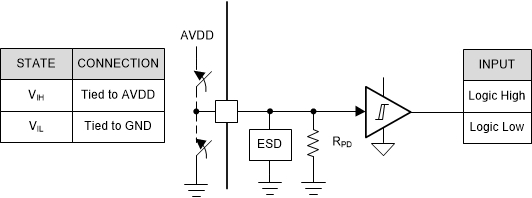
Figure 8-23 shows the input structure for the logic level pins, BRAKE, DIR, DRVOFF, nSLEEP, PWM, SCLK and SDI. The input can be with a voltage or external resistor. It is recommended to put these pins low in device sleep mode to reduce leakage current through internal pull-down resistors.
 Figure 8-23 Logic-Level Input Pin Structure