ZHCS136B November 2010 – June 2018 MSP430AFE221 , MSP430AFE222 , MSP430AFE223 , MSP430AFE231 , MSP430AFE232 , MSP430AFE233 , MSP430AFE251 , MSP430AFE252 , MSP430AFE253
PRODUCTION DATA.
- 1器件概述
- 2修订历史记录
- 3Device Comparison
- 4Terminal Configuration and Functions
-
5Specifications
- 5.1 Absolute Maximum Ratings
- 5.2 ESD Ratings
- 5.3 Recommended Operating Conditions
- 5.4 Thermal Resistance Characteristics for PW-24 Package
- 5.5 Active Mode Supply Current (Into DVCC and AVCC) Excluding External Current
- 5.6 Typical Characteristics – Active-Mode Supply Current (Into DVCC and AVCC)
- 5.7 Low-Power-Mode Supply Currents (Into VCC) Excluding External Current
- 5.8 Typical Characteristics – LPM4 Current
- 5.9 Schmitt-Trigger Inputs (Ports Px and RST/NMI)
- 5.10 Leakage Current (Ports Px)
- 5.11 Outputs (Ports Px)
- 5.12 Output Frequency (Ports Px)
- 5.13 Typical Characteristics – Outputs
- 5.14 POR, BOR
- 5.15 Typical Characteristics – POR, BOR
- 5.16 Supply Voltage Supervisor (SVS), Supply Voltage Monitor (SVM)
- 5.17 Main DCO Characteristics
- 5.18 DCO Frequency
- 5.19 Calibrated DCO Frequencies – Tolerance
- 5.20 Wake-up Times From Lower-Power Modes (LPM3, LPM4)
- 5.21 Typical Characteristics – DCO Clock Wake-up Time
- 5.22 Internal Very-Low-Power Low-Frequency Oscillator (VLO)
- 5.23 Crystal Oscillator (XT2)
- 5.24 Typical Characteristics – XT2 Oscillator
- 5.25 SD24_A, Power Supply
- 5.26 SD24_A, Input Range
- 5.27 SD24_A, Performance
- 5.28 SD24_A, Temperature Sensor and Built-In VCC Sense
- 5.29 SD24_A, Built-In Voltage Reference
- 5.30 SD24_A, Reference Output Buffer
- 5.31 SD24_A, External Reference Input
- 5.32 USART0
- 5.33 Timer_A3
- 5.34 Flash Memory
- 5.35 RAM
- 5.36 JTAG and Spy-Bi-Wire Interface
- 5.37 JTAG Fuse
-
6Detailed Description
- 6.1 CPU
- 6.2 Instruction Set
- 6.3 Operating Modes
- 6.4 Interrupt Vector Addresses
- 6.5 Special Function Registers
- 6.6 Memory Organization
- 6.7 Flash Memory
- 6.8 Peripherals
- 6.9 Oscillator and System Clock
- 6.10 Brownout, Supply Voltage Supervisor
- 6.11 Digital I/O
- 6.12 Watchdog Timer (WDT+)
- 6.13 Timer_A3
- 6.14 USART0
- 6.15 Hardware Multiplier
- 6.16 SD24_A
- 6.17 Peripheral File Map
- 6.18
I/O Port Schematics
- 6.18.1 Port P1 Pin Schematic: P1.0 Input/Output With Schmitt Trigger
- 6.18.2 Port P1 Pin Schematic: P1.1 and P1.2 Input/Output With Schmitt Trigger
- 6.18.3 Port P1 Pin Schematic: P1.3 Input/Output With Schmitt Trigger
- 6.18.4 Port P1 Pin Schematic: P1.4 Input/Output With Schmitt Trigger
- 6.18.5 Port P1 Pin Schematic: P1.5 to P1.7 Input/Output With Schmitt Trigger
- 6.18.6 Port P2 Pin Schematic: P2.0 Input/Output With Schmitt Trigger
- 6.18.7 Port P2 Pin Schematic: P2.6, Input/Output With Schmitt Trigger
- 6.18.8 Port P2 Pin Schematic: P2.7, Input/Output With Schmitt Trigger
- 6.18.9 JTAG Fuse Check Mode
- 7器件和文档支持
- 8机械、封装和可订购信息
6.18.4 Port P1 Pin Schematic: P1.4 Input/Output With Schmitt Trigger
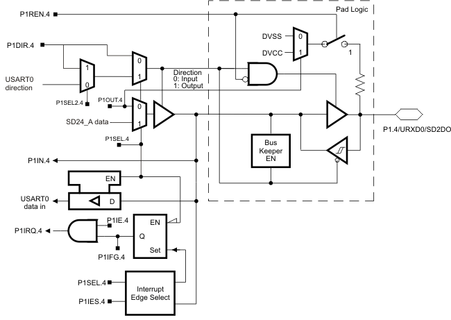
Figure 6-11 shows the port schematic. Table 6-15 summarizes the selection of the pin functions.
 Figure 6-11 Port P1 (P1.4) Schematic
 Table 6-15 Port P1 (P1.4) Pin Functions
| PIN NAME (P1.x) | x | FUNCTION | CONTROL BITS OR SIGNALS(1) | ||
|---|---|---|---|---|---|
| P1DIR.x | P1SEL.x | P1SEL2.x | |||
| P1.4/URXD0/SD2DO | 4 | P1.4 (I/O) | I: 0, O: 1 | 0 | X |
| URXD0 | X | 1 | 0 | ||
| SD2DO | 1 | 1 | 1 | ||
(1) X = don't care