ZHCS406R August 2010 – September 2018 MSP430F5131 , MSP430F5132 , MSP430F5151 , MSP430F5152 , MSP430F5171 , MSP430F5172
PRODUCTION DATA.
- 1器件概述
- 2修订历史记录
- 3Device Comparison
- 4Terminal Configuration and Functions
-
5Specifications
- 5.1 Absolute Maximum Ratings
- 5.2 ESD Ratings
- 5.3 Recommended Operating Conditions
- 5.4 Active Mode Supply Current Into VCC Excluding External Current
- 5.5 Low-Power Mode Supply Currents (Into VCC) Excluding External Current
- 5.6 Thermal Resistance Characteristics
- 5.7 Schmitt-Trigger Inputs – General-Purpose I/O (P1.0 to P1.5, P3.2 to P3.7, and PJ.0 to PJ.6)
- 5.8 Schmitt-Trigger Inputs – General-Purpose I/O (P1.6 and P1.7, P2.0 to P2.7, and P3.0 and P3.1)
- 5.9 Inputs – Ports P1 and P2
- 5.10 Leakage Current – General-Purpose I/O
- 5.11 Outputs – Ports P1, P3, PJ (Full Drive Strength, P1.0 to P1.5, P3.2 to P3.7, PJ.0 to PJ.6)
- 5.12 Outputs – Ports P1 to P3 (Full Drive Strength, P1.6 and P1.7, P2.0 to P2.7, P3.0 and P3.1)
- 5.13 Outputs – Ports P1, P3, PJ (Reduced Drive Strength, P1.0 to P1.5, P3.2 to P3.7, PJ.0 to PJ.6)
- 5.14 Outputs – Ports P1 to P3 (Reduced Drive Strength, P1.6 and P1.7, P2.0 to P2.7, P3.0 and P3.1)
- 5.15 Output Frequency – Ports P1.0 to P1.5, P3.2 to P3.7, PJ.0 to PJ.6
- 5.16 Output Frequency – Ports P1.6 and P1.7, P2.0 to P2.7, P3.0 and P3.1
- 5.17 Typical Characteristics – Outputs, Reduced Drive Strength (PxDS.y = 0), Ports P1.0 to P1.5, P3.2 to P3.7, PJ.0 to PJ.6
- 5.18 Typical Characteristics – Outputs, Full Drive Strength (PxDS.y = 1), Ports P1.0 to P1.5, P3.2 to P3.7, PJ.0 to PJ.6
- 5.19 Typical Characteristics – Outputs, Reduced Drive Strength (PxDS.y = 0), Ports P1.6 and P1.7, P2.0 to P2.7, P3.0 and P3.1
- 5.20 Typical Characteristics – Outputs, Full Drive Strength (PxDS.y = 1), Ports P1.6 and P1.7, P2.0 to P2.7, P3.0 and P3.1
- 5.21 Crystal Oscillator, XT1, Low-Frequency Mode
- 5.22 Crystal Oscillator, XT1, High-Frequency Mode
- 5.23 Internal Very-Low-Power Low-Frequency Oscillator (VLO)
- 5.24 Internal Reference, Low-Frequency Oscillator (REFO)
- 5.25 DCO Frequency
- 5.26 PMM, Brownout Reset (BOR)
- 5.27 PMM, Core Voltage
- 5.28 PMM, SVS High Side
- 5.29 PMM, SVM High Side
- 5.30 PMM, SVS Low Side
- 5.31 PMM, SVM Low Side
- 5.32 Wake-up Times From Low-Power Modes
- 5.33 Timer_A
- 5.34 USCI (UART Mode)
- 5.35 USCI (SPI Master Mode)
- 5.36 USCI (SPI Slave Mode)
- 5.37 USCI (I2C Mode)
- 5.38 10-Bit ADC, Power Supply and Input Range Conditions (MSP430F51x2 Devices Only)
- 5.39 10-Bit ADC, Timing Parameters (MSP430F51x2 Devices Only)
- 5.40 10-Bit ADC, Linearity Parameters (MSP430F51x2 Devices Only)
- 5.41 REF, External Reference (MSP430F51x2 Devices Only)
- 5.42 REF, Built-In Reference (MSP430F51x2 Devices Only)
- 5.43 Comparator_B
- 5.44 Timer_D, Power Supply and Reference Clock
- 5.45 Timer_D, Local Clock Generator Frequency
- 5.46 Timer_D, Trimmed Clock Frequencies
- 5.47 Timer_D, Frequency Multiplication Mode
- 5.48 Timer_D, Input Capture and Output Compare Timing
- 5.49 Flash Memory
- 5.50 JTAG and Spy-Bi-Wire Interface
-
6Detailed Description
- 6.1 CPU
- 6.2 Instruction Set
- 6.3 Operating Modes
- 6.4 Interrupt Vector Addresses
- 6.5 Memory Organization
- 6.6 Bootloader (BSL)
- 6.7 Flash Memory
- 6.8 RAM
- 6.9
Peripherals
- 6.9.1 Digital I/O
- 6.9.2 Port Mapping Controller
- 6.9.3 Oscillator and System Clock
- 6.9.4 Power-Management Module (PMM)
- 6.9.5 Hardware Multiplier
- 6.9.6 Watchdog Timer (WDT_A)
- 6.9.7 System Module (SYS)
- 6.9.8 DMA Controller
- 6.9.9 Universal Serial Communication Interface (USCI)
- 6.9.10 TA0
- 6.9.11 TD0
- 6.9.12 TD1
- 6.9.13 Comparator_B
- 6.9.14 ADC10_A (MSP430F51x2 Only)
- 6.9.15 CRC16
- 6.9.16 Reference (REF) Module Voltage Reference
- 6.9.17 Embedded Emulation Module (EEM) (S Version)
- 6.9.18 Peripheral File Map
- 6.10
Input/Output Diagrams
- 6.10.1 Port P1 (P1.0 to P1.5) Input/Output With Schmitt Trigger
- 6.10.2 Port P1 (P1.6 to P1.7) Input/Output With Schmitt Trigger
- 6.10.3 Port P2 (P2.0 to P2.7) Input/Output With Schmitt Trigger
- 6.10.4 Port P3 (P3.0 and P3.1) Input/Output With Schmitt Trigger
- 6.10.5 Port P3 (P3.2 and P3.3) Input/Output With Schmitt Trigger
- 6.10.6 Port P3 (P3.4) Input/Output With Schmitt Trigger
- 6.10.7 Port P3 (P3.5) Input/Output With Schmitt Trigger
- 6.10.8 Port P3 (P3.6) Input/Output With Schmitt Trigger
- 6.10.9 Port P3 (P3.7) Input/Output With Schmitt Trigger
- 6.10.10 Port J (PJ.0) JTAG Pin TDO, Input/Output With Schmitt Trigger or Output
- 6.10.11 Port J (PJ.1 to PJ.3) JTAG Pins TMS, TCK, TDI/TCLK, Input/Output With Schmitt Trigger or Output
- 6.10.12 Port J (PJ.4) Input/Output With Schmitt Trigger
- 6.10.13 Port J (PJ.5) Input/Output With Schmitt Trigger
- 6.10.14 Port J (PJ.6) Input/Output With Schmitt Trigger
- 6.11 Device Descriptors
- 7器件和文档支持
- 8机械、封装和可订购信息
封装选项
机械数据 (封装 | 引脚)
散热焊盘机械数据 (封装 | 引脚)
订购信息
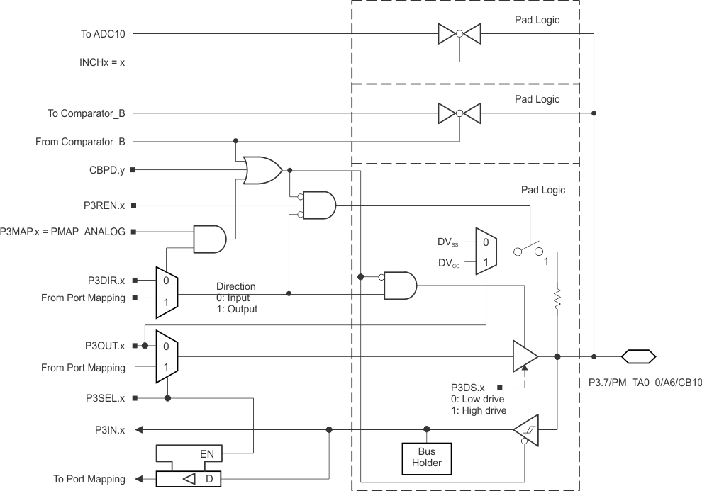
6.10.9 Port P3 (P3.7) Input/Output With Schmitt Trigger
Figure 6-10 shows the port diagram. Table 6-52 summarizes the selection of the pin function.
 Figure 6-10 Port P3 (P3.7) Diagram
 Table 6-52 Port P3 (P3.7) Pin Functions
| PIN NAME (P3.x) | x | FUNCTION | CONTROL BITS OR SIGNALS(1) | |||
|---|---|---|---|---|---|---|
| P3DIR.x | P3SEL.2 | P3MAP.x | CBPD.y | |||
| P3.7/ | 7 | P3.x (I/O)(1) | I: 0; O: 1 | 0 | X | 0 |
| PM_TA0.0/ | TA0.CCR0 | 0 | 1 | default | 0 | |
| TA0.TA0 | 1 | 1 | default | 0 | ||
| A6/ | A6(2) | X | 1 | 31
INCHx = 6 |
X | |
| CB10 | CB10 | X | X | 0 | 1 (y = 10) | |
(1) X = Don't care
(2) MSP430F51x2 devices only.