ZHCSDE8A February 2015 – October 2018 MSP430F67621A , MSP430F67641A
PRODUCTION DATA.
- 1器件概述
- 2修订历史记录
- 3Device Comparison
- 4Terminal Configuration and Functions
-
5Specifications
- 5.1 Absolute Maximum Ratings
- 5.2 ESD Ratings
- 5.3 Recommended Operating Conditions
- 5.4 Active Mode Supply Current Into VCC Excluding External Current
- 5.5 Low-Power Mode Supply Currents (Into VCC) Excluding External Current
- 5.6 Low-Power Mode With LCD Supply Currents (Into VCC) Excluding External Current
- 5.7 Thermal Resistance Characteristics
- 5.8
Timing and Switching Characteristics
- 5.8.1 Power Supply Sequencing
- 5.8.2 Reset Timing
- 5.8.3 Clock Specifications
- 5.8.4
Digital I/O Ports
- Table 5-6 Schmitt-Trigger Inputs, General-Purpose I/O
- Table 5-7 Inputs, Ports P1 and P2
- Table 5-8 Leakage Current, General-Purpose I/O
- Table 5-9 Outputs, General-Purpose I/O (Full Drive Strength)
- 5.8.4.1 Typical Characteristics, General-Purpose I/O (Full Drive Strength)
- Table 5-10 Outputs, General-Purpose I/O (Reduced Drive Strength)
- 5.8.4.2 Typical Characteristics, General-Purpose I/O (Reduced Drive Strength)
- Table 5-11 Output Frequency, General-Purpose I/O
- 5.8.5 Power-Management Module (PMM)
- 5.8.6
Auxiliary Supplies Module
- Table 5-18 Auxiliary Supplies, Recommended Operating Conditions
- Table 5-19 Auxiliary Supplies, AUX3 (Backup Subsystem) Currents
- Table 5-20 Auxiliary Supplies, Auxiliary Supply Monitor
- Table 5-21 Auxiliary Supplies, Switch ON-Resistance
- Table 5-22 Auxiliary Supplies, Switching Time
- Table 5-23 Auxiliary Supplies, Switch Leakage
- Table 5-24 Auxiliary Supplies, Auxiliary Supplies to ADC10_A
- Table 5-25 Auxiliary Supplies, Charge-Limiting Resistor
- 5.8.7 Timer_A Module
- 5.8.8 eUSCI Module
- 5.8.9 LCD Controller
- 5.8.10
SD24_B Module
- Table 5-35 SD24_B Power Supply and Recommended Operating Conditions
- Table 5-36 SD24_B Analog Input
- Table 5-37 SD24_B Supply Currents
- Table 5-38 SD24_B Performance
- Table 5-39 SD24_B AC Performance
- Table 5-40 SD24_B AC Performance
- Table 5-41 SD24_B AC Performance
- Table 5-42 SD24_B External Reference Input
- 5.8.11 ADC10_A Module
- 5.8.12 REF Module
- 5.8.13 Flash
- 5.8.14 Emulation and Debug
-
6Detailed Description
- 6.1 Overview
- 6.2 Functional Block Diagrams
- 6.3 CPU
- 6.4 Instruction Set
- 6.5 Operating Modes
- 6.6 Interrupt Vector Addresses
- 6.7 Bootloader (BSL)
- 6.8 JTAG Operation
- 6.9 Flash Memory
- 6.10 RAM
- 6.11 Backup RAM
- 6.12
Peripherals
- 6.12.1 Oscillator and System Clock
- 6.12.2 Power-Management Module (PMM)
- 6.12.3 Auxiliary Supply System
- 6.12.4 Backup Subsystem
- 6.12.5 Digital I/O
- 6.12.6 Port Mapping Controller
- 6.12.7 System Module (SYS)
- 6.12.8 Watchdog Timer (WDT_A)
- 6.12.9 DMA Controller
- 6.12.10 CRC16
- 6.12.11 Hardware Multiplier
- 6.12.12 Enhanced Universal Serial Communication Interface (eUSCI)
- 6.12.13 ADC10_A
- 6.12.14 SD24_B
- 6.12.15 TA0
- 6.12.16 TA1
- 6.12.17 TA2
- 6.12.18 TA3
- 6.12.19 SD24_B Triggers
- 6.12.20 ADC10_A Triggers
- 6.12.21 Real-Time Clock (RTC_C)
- 6.12.22 Reference (REF) Module Voltage Reference
- 6.12.23 LCD_C
- 6.12.24 Embedded Emulation Module (EEM) (S Version)
- 6.13
Input/Output Diagrams
- 6.13.1 Port P1 (P1.0 and P1.1) Input/Output With Schmitt Trigger
- 6.13.2 Port P1 (P1.2) Input/Output With Schmitt Trigger
- 6.13.3 Port P1 (P1.3 to P1.5) Input/Output With Schmitt Trigger
- 6.13.4 Port P1 (P1.6 and P1.7), Port P2 (P2.0 and P2.1) (PZ Package Only) Input/Output With Schmitt Trigger
- 6.13.5 Port P2 (P2.2 to P2.7) Input/Output With Schmitt Trigger (PZ Package Only)
- 6.13.6 Port P3 (P3.0 to P3.3) Input/Output With Schmitt Trigger (PZ Package Only)
- 6.13.7 Port P3 (P3.4 to P3.7) Input/Output With Schmitt Trigger (PZ Package Only)
- 6.13.8 Port P4 (P4.0 to P4.7), Port P5 (P5.0 to P5.7), Port P6 (P6.0 to P6.7), Port P7 (P7.0 to P7.7), Port P8 (P8.0 to P8.3) Input/Output With Schmitt Trigger (PZ Package Only)
- 6.13.9 Port P8 (P8.4 to P8.7) Input/Output With Schmitt Trigger (PZ Package Only)
- 6.13.10 Port P9 (P9.0), Input/Output With Schmitt Trigger (PZ Package Only)
- 6.13.11 Port P9 (P9.1 to P9.3) Input/Output With Schmitt Trigger (PZ Package Only)
- 6.13.12 Port P2 (P2.0 and P2.1) Input/Output With Schmitt Trigger (PN Package Only)
- 6.13.13 Port P2 (P2.2 to P2.7) Input/Output With Schmitt Trigger (PN Package Only)
- 6.13.14 Port P3 (P3.0 to P3.7) Input/Output With Schmitt Trigger (PN Package Only)
- 6.13.15 Port P4 (P4.0 to P4.7), Port P5 (P5.0 to P5.7), Port P6 (P6.0 to P6.7) Input/Output With Schmitt Trigger (PN Package Only)
- 6.13.16 Port PJ (PJ.0) JTAG Pin TDO, Input/Output With Schmitt Trigger or Output
- 6.13.17 Port PJ (PJ.1 to PJ.3) JTAG Pins TMS, TCK, TDI/TCLK, Input/Output With Schmitt Trigger or Output
- 6.14 Device Descriptors (TLV)
- 6.15 Memory
- 6.16 Identification
- 7Applications, Implementation, and Layout
- 8器件和文档支持
- 9机械、封装和可订购信息
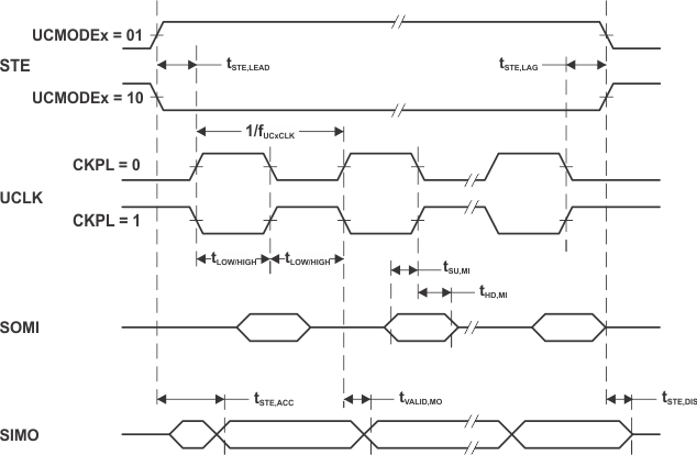
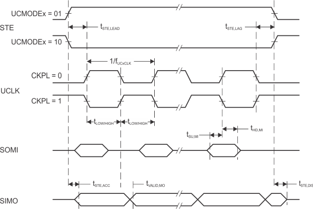
Table 5-30 eUSCI (SPI Master Mode) Switching Characteristics
over recommended ranges of supply voltage and operating free-air temperature (unless otherwise noted)(1)| PARAMETER | TEST CONDITIONS | VCC | MIN | MAX | UNIT | |
|---|---|---|---|---|---|---|
| tSTE,LEAD | STE lead time, STE active to clock | UCSTEM = 0, UCMODEx = 01 or 10 | 2 V, 3 V | 150 | ns | |
| UCSTEM = 1, UCMODEx = 01 or 10 | 2 V, 3 V | 150 | ||||
| tSTE,LAG | STE lag time, Last clock to STE inactive | UCSTEM = 0, UCMODEx = 01 or 10 | 2 V, 3 V | 200 | ns | |
| UCSTEM = 1, UCMODEx = 01 or 10 | 2 V, 3 V | 200 | ||||
| tSTE,ACC | STE access time, STE active to SIMO data out | UCSTEM = 0, UCMODEx = 01 or 10 | 2 V | 50 | ns | |
| 3 V | 30 | |||||
| UCSTEM = 1, UCMODEx = 01 or 10 | 2 V | 50 | ||||
| 3 V | 30 | |||||
| tSTE,DIS | STE disable time, STE inactive to SIMO high impedance | UCSTEM = 0, UCMODEx = 01 or 10 | 2 V | 40 | ns | |
| 3 V | 25 | |||||
| UCSTEM = 1, UCMODEx = 01 or 10 | 2 V | 40 | ||||
| 3 V | 25 | |||||
| tSU,MI | SOMI input data setup time | 2 V | 50 | ns | ||
| 3 V | 30 | |||||
| tHD,MI | SOMI input data hold time | 2 V | 0 | ns | ||
| 3 V | 0 | |||||
| tVALID,MO | SIMO output data valid time(2) | UCLK edge to SIMO valid, CL = 20 pF | 2 V | 9 | ns | |
| 3 V | 5 | |||||
| tHD,MO | SIMO output data hold time(3) | CL = 20 pF | 2 V | 0 | ns | |
| 3 V | 0 | |||||
(1) fUCxCLK = 1/2tLO/HI with tLO/HI = max(tVALID,MO(eUSCI) + tSU,SI(Slave), tSU,MI(eUSCI) + tVALID,SO(Slave))
For the slave parameters tSU,SI(Slave) and tVALID,SO(Slave), see the SPI parameters of the attached slave.
For the slave parameters tSU,SI(Slave) and tVALID,SO(Slave), see the SPI parameters of the attached slave.
(2) Specifies the time to drive the next valid data to the SIMO output after the output changing UCLK clock edge. See the timing diagrams in Figure 5-13 and Figure 5-14.
(3) Specifies how long data on the SIMO output is valid after the output changing UCLK clock edge. Negative values indicate that the data on the SIMO output can become invalid before the output changing clock edge observed on UCLK. See the timing diagrams in Figure 5-13 and Figure 5-14.
 Figure 5-13 BadDriveBacuSPI Master Mode, CKPH = 0
  Figure 5-14 SPI Master Mode, CKPH = 1
 Table 5-31 lists the switching characteristics of the eUSCI in SPI slave mode.