ZHCSDO6B May 2015 – September 2020 MSP430FG6425 , MSP430FG6426 , MSP430FG6625 , MSP430FG6626
PRODUCTION DATA
- 1 特性
- 2 应用
- 3 说明
- 4 功能方框图
- 5 Revision History
- 6 Device Comparison
- 7 Terminal Configuration and Functions
-
8 Specifications
- 8.1 Absolute Maximum Ratings
- 8.2 ESD Ratings
- 8.3 Recommended Operating Conditions
- 8.4 Active Mode Supply Current Into VCC Excluding External Current
- 8.5 Low-Power Mode Supply Currents (Into VCC) Excluding External Current
- 8.6 Low-Power Mode With LCD Supply Currents (Into VCC) Excluding External Current
- 8.7 Thermal Resistance Characteristics
- 8.8
Timing and Switching Characteristics
- 8.8.1 Power Supply Sequencing
- 8.8.2 Reset Timing
- 8.8.3 Clock Specifications
- 8.8.4 Wake-up Characteristics
- 8.8.5
General-Purpose I/Os
- 8.8.5.1 Schmitt-Trigger Inputs – General-Purpose I/O
- 8.8.5.2 Inputs – Ports P1, P2, P3, and P4
- 8.8.5.3 Leakage Current – General-Purpose I/O
- 8.8.5.4 Outputs – General-Purpose I/O (Full Drive Strength)
- 8.8.5.5 Outputs – General-Purpose I/O (Reduced Drive Strength)
- 8.8.5.6 Output Frequency – Ports P1, P2 and P3
- 8.8.5.7 Typical Characteristics – Outputs, Reduced Drive Strength (PxDS.y = 0)
- 8.8.5.8 Typical Characteristics – Outputs, Full Drive Strength (PxDS.y = 1)
- 8.8.6 PMM
- 8.8.7 Timers
- 8.8.8 Battery Backup
- 8.8.9 USCI
- 8.8.10 LCD Controller
- 8.8.11 CTSD16
- 8.8.12 REF
- 8.8.13 DAC
- 8.8.14 Operational Amplifier
- 8.8.15 Switches
- 8.8.16 Comparator
- 8.8.17 USB
- 8.8.18 LDO-PWR (LDO Power System)
- 8.8.19 Flash
- 8.8.20 Debug and Emulation
-
9 Detailed Description
- 9.1 Overview
- 9.2 CPU
- 9.3 Instruction Set
- 9.4 Operating Modes
- 9.5 Interrupt Vector Addresses
- 9.6 USB BSL
- 9.7 UART BSL
- 9.8 JTAG Operation
- 9.9 Flash Memory
- 9.10 RAM
- 9.11 Backup RAM
- 9.12
Peripherals
- 9.12.1 Digital I/O
- 9.12.2 Port Mapping Controller
- 9.12.3 Oscillator and System Clock
- 9.12.4 Power Management Module (PMM)
- 9.12.5 Hardware Multiplier (MPY32)
- 9.12.6 Real-Time Clock (RTC_B)
- 9.12.7 Watchdog Timer (WDT_A)
- 9.12.8 System Module (SYS)
- 9.12.9 DMA Controller
- 9.12.10 Universal Serial Communication Interface (USCI)
- 9.12.11 Timer TA0
- 9.12.12 Timer TA1
- 9.12.13 Timer TA2
- 9.12.14 Timer TB0
- 9.12.15 Comparator_B
- 9.12.16 Signal Chain
- 9.12.17 REF Voltage Reference
- 9.12.18 CRC16
- 9.12.19 LCD_B
- 9.12.20 USB Universal Serial Bus
- 9.12.21 LDO and PU Port
- 9.12.22 Embedded Emulation Module (EEM) (L Version)
- 9.13
Input/Output Diagrams
- 9.13.1 Port P1 (P1.0 to P1.7) Input/Output With Schmitt Trigger
- 9.13.2 Port P2 (P2.0 to P2.7) Input/Output With Schmitt Trigger
- 9.13.3 Port P3 (P3.0 to P3.7) Input/Output With Schmitt Trigger
- 9.13.4 Port P4 (P4.0 to P4.7) Input/Output With Schmitt Trigger
- 9.13.5 Port P5 (P5.0) Input/Output With Schmitt Trigger
- 9.13.6 Port P5 (P5.1 and P5.6) Input/Output With Schmitt Trigger
- 9.13.7 Port P5 (P5.3 to P5.5, P5.7) Input/Output With Schmitt Trigger
- 9.13.8 Port P6 (P6.0 to P6.1) Input/Output With Schmitt Trigger
- 9.13.9 Port P6 (P6.2 and P6.3) Input/Output With Schmitt Trigger
- 9.13.10 Port P6 (P6.4) Input/Output With Schmitt Trigger
- 9.13.11 Port P6 (P6.5) Input/Output With Schmitt Trigger
- 9.13.12 Port P6 (P6.6) Input/Output With Schmitt Trigger
- 9.13.13 Port P6 (P6.7) Input/Output With Schmitt Trigger
- 9.13.14 Port P7 (P7.2 and P7.3) Input/Output With Schmitt Trigger
- 9.13.15 Port P7 (P7.4) Input/Output With Schmitt Trigger
- 9.13.16 Port P7 (P7.5) Input/Output With Schmitt Trigger
- 9.13.17 Port P7 (P7.6) Input/Output With Schmitt Trigger
- 9.13.18 Port P7 (P7.7) Input/Output With Schmitt Trigger
- 9.13.19 Port P8 (P8.0 to P8.7) Input/Output With Schmitt Trigger
- 9.13.20 Port P9 (P9.0 to P9.7) Input/Output With Schmitt Trigger
- 9.13.21 Port U (PU.0/DP, PU.1/DM, PUR) USB Ports for MSP430FG662x
- 9.13.22 Port J (J.0) JTAG Pin TDO, Input/Output With Schmitt Trigger or Output
- 9.13.23 Port J (J.1 to J.3) JTAG Pins TMS, TCK, TDI/TCLK, Input/Output With Schmitt Trigger or Output
- 9.14 Device Descriptors
- 9.15 Memory
- 9.16 Identification
-
10Applications, Implementation, and Layout
- 10.1 Device Connection and Layout Fundamentals
- 10.2
Peripheral- and Interface-Specific Design Information
- 10.2.1 CTSD16 Peripheral
- 10.2.2 Operational Amplifier With Ground Switches Peripheral
- 10.2.3 RTC_B With Battery Backup System
- 10.2.4 LCD_B Peripheral
- 10.2.5 DAC12 Peripheral
- 10.2.6 USB Module
- 10.2.7 LDO Module
- 11Device and Documentation Support
- 12Mechanical, Packaging, and Orderable Information
9.13.10 Port P6 (P6.4) Input/Output With Schmitt Trigger
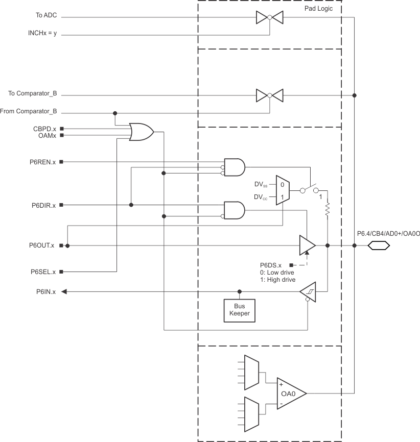
Figure 9-12 shows the port diagram. Table 9-25 summarizes the selection of the port function.
 Figure 9-12 Port P6 (P6.4) Diagram
Table 9-25 Port P6 (P6.4) Pin Functions
| PIN NAME (P6.x) | x | FUNCTION | CONTROL BITS OR SIGNALS(1) | |||
|---|---|---|---|---|---|---|
| P6DIR.x | P6SEL.x(3) | CBPD.x(3) | OAMx | |||
| P6.4/CB4/AD0+/OA0O | 4 | P6.4 (I/O) | I: 0; O: 1 | 0 | 0 | 0(4) |
| CB4 | X | X | 1 | 0(4) | ||
| AD0+ (2) | X | 1 | X | 0(4) | ||
| OA0O | X | X | X | = 1(4) | ||
(1) X = Don't care
(2) The ADC channel Ax is connected internally to AVSS if not selected by the respective INCHx bits.
(3) Setting the P6SEL.x bit, the CBPD.x bit, or the OAMx bit disables the output driver and the input Schmitt trigger to prevent parasitic cross currents when applying analog signals.
(4) Setting OAMx = 0 disables the operational amplifier and its output is high impedance. Setting OAMx = 1 enables the operational amplifier output. Because the operational amplifier output is shared with the ADC channel, selection of the respective ADC channel allows for direct measurement of the output voltage of the amplifier.