ZHCSDO6B May 2015 – September 2020 MSP430FG6425 , MSP430FG6426 , MSP430FG6625 , MSP430FG6626
PRODUCTION DATA
- 1 特性
- 2 应用
- 3 说明
- 4 功能方框图
- 5 Revision History
- 6 Device Comparison
- 7 Terminal Configuration and Functions
-
8 Specifications
- 8.1 Absolute Maximum Ratings
- 8.2 ESD Ratings
- 8.3 Recommended Operating Conditions
- 8.4 Active Mode Supply Current Into VCC Excluding External Current
- 8.5 Low-Power Mode Supply Currents (Into VCC) Excluding External Current
- 8.6 Low-Power Mode With LCD Supply Currents (Into VCC) Excluding External Current
- 8.7 Thermal Resistance Characteristics
- 8.8
Timing and Switching Characteristics
- 8.8.1 Power Supply Sequencing
- 8.8.2 Reset Timing
- 8.8.3 Clock Specifications
- 8.8.4 Wake-up Characteristics
- 8.8.5
General-Purpose I/Os
- 8.8.5.1 Schmitt-Trigger Inputs – General-Purpose I/O
- 8.8.5.2 Inputs – Ports P1, P2, P3, and P4
- 8.8.5.3 Leakage Current – General-Purpose I/O
- 8.8.5.4 Outputs – General-Purpose I/O (Full Drive Strength)
- 8.8.5.5 Outputs – General-Purpose I/O (Reduced Drive Strength)
- 8.8.5.6 Output Frequency – Ports P1, P2 and P3
- 8.8.5.7 Typical Characteristics – Outputs, Reduced Drive Strength (PxDS.y = 0)
- 8.8.5.8 Typical Characteristics – Outputs, Full Drive Strength (PxDS.y = 1)
- 8.8.6 PMM
- 8.8.7 Timers
- 8.8.8 Battery Backup
- 8.8.9 USCI
- 8.8.10 LCD Controller
- 8.8.11 CTSD16
- 8.8.12 REF
- 8.8.13 DAC
- 8.8.14 Operational Amplifier
- 8.8.15 Switches
- 8.8.16 Comparator
- 8.8.17 USB
- 8.8.18 LDO-PWR (LDO Power System)
- 8.8.19 Flash
- 8.8.20 Debug and Emulation
-
9 Detailed Description
- 9.1 Overview
- 9.2 CPU
- 9.3 Instruction Set
- 9.4 Operating Modes
- 9.5 Interrupt Vector Addresses
- 9.6 USB BSL
- 9.7 UART BSL
- 9.8 JTAG Operation
- 9.9 Flash Memory
- 9.10 RAM
- 9.11 Backup RAM
- 9.12
Peripherals
- 9.12.1 Digital I/O
- 9.12.2 Port Mapping Controller
- 9.12.3 Oscillator and System Clock
- 9.12.4 Power Management Module (PMM)
- 9.12.5 Hardware Multiplier (MPY32)
- 9.12.6 Real-Time Clock (RTC_B)
- 9.12.7 Watchdog Timer (WDT_A)
- 9.12.8 System Module (SYS)
- 9.12.9 DMA Controller
- 9.12.10 Universal Serial Communication Interface (USCI)
- 9.12.11 Timer TA0
- 9.12.12 Timer TA1
- 9.12.13 Timer TA2
- 9.12.14 Timer TB0
- 9.12.15 Comparator_B
- 9.12.16 Signal Chain
- 9.12.17 REF Voltage Reference
- 9.12.18 CRC16
- 9.12.19 LCD_B
- 9.12.20 USB Universal Serial Bus
- 9.12.21 LDO and PU Port
- 9.12.22 Embedded Emulation Module (EEM) (L Version)
- 9.13
Input/Output Diagrams
- 9.13.1 Port P1 (P1.0 to P1.7) Input/Output With Schmitt Trigger
- 9.13.2 Port P2 (P2.0 to P2.7) Input/Output With Schmitt Trigger
- 9.13.3 Port P3 (P3.0 to P3.7) Input/Output With Schmitt Trigger
- 9.13.4 Port P4 (P4.0 to P4.7) Input/Output With Schmitt Trigger
- 9.13.5 Port P5 (P5.0) Input/Output With Schmitt Trigger
- 9.13.6 Port P5 (P5.1 and P5.6) Input/Output With Schmitt Trigger
- 9.13.7 Port P5 (P5.3 to P5.5, P5.7) Input/Output With Schmitt Trigger
- 9.13.8 Port P6 (P6.0 to P6.1) Input/Output With Schmitt Trigger
- 9.13.9 Port P6 (P6.2 and P6.3) Input/Output With Schmitt Trigger
- 9.13.10 Port P6 (P6.4) Input/Output With Schmitt Trigger
- 9.13.11 Port P6 (P6.5) Input/Output With Schmitt Trigger
- 9.13.12 Port P6 (P6.6) Input/Output With Schmitt Trigger
- 9.13.13 Port P6 (P6.7) Input/Output With Schmitt Trigger
- 9.13.14 Port P7 (P7.2 and P7.3) Input/Output With Schmitt Trigger
- 9.13.15 Port P7 (P7.4) Input/Output With Schmitt Trigger
- 9.13.16 Port P7 (P7.5) Input/Output With Schmitt Trigger
- 9.13.17 Port P7 (P7.6) Input/Output With Schmitt Trigger
- 9.13.18 Port P7 (P7.7) Input/Output With Schmitt Trigger
- 9.13.19 Port P8 (P8.0 to P8.7) Input/Output With Schmitt Trigger
- 9.13.20 Port P9 (P9.0 to P9.7) Input/Output With Schmitt Trigger
- 9.13.21 Port U (PU.0/DP, PU.1/DM, PUR) USB Ports for MSP430FG662x
- 9.13.22 Port J (J.0) JTAG Pin TDO, Input/Output With Schmitt Trigger or Output
- 9.13.23 Port J (J.1 to J.3) JTAG Pins TMS, TCK, TDI/TCLK, Input/Output With Schmitt Trigger or Output
- 9.14 Device Descriptors
- 9.15 Memory
- 9.16 Identification
-
10Applications, Implementation, and Layout
- 10.1 Device Connection and Layout Fundamentals
- 10.2
Peripheral- and Interface-Specific Design Information
- 10.2.1 CTSD16 Peripheral
- 10.2.2 Operational Amplifier With Ground Switches Peripheral
- 10.2.3 RTC_B With Battery Backup System
- 10.2.4 LCD_B Peripheral
- 10.2.5 DAC12 Peripheral
- 10.2.6 USB Module
- 10.2.7 LDO Module
- 11Device and Documentation Support
- 12Mechanical, Packaging, and Orderable Information
8.8.14.1 Operational Amplifier, OA0, OA1, PGA Buffers
over operating free-air temperature range (unless otherwise noted)
| PARAMETER | TEST CONDITIONS | VCC | MIN | TYP | MAX | UNIT | |
|---|---|---|---|---|---|---|---|
| VCC | Analog supply voltage | AVCC = DVCC, AVSS = DVSS = 0 V | 2.2 | 3.6 | V | ||
| CCPCAP | External charge pump capacitor to AVSS. | Required when charge pump is enabled | 20 | 22 | 24 | nF | |
| ICP_PEAK | Charge pump peak current | OARRI = 0h to 1h, ICP_LOAD = 0 μA |
1.6 | mA | |||
| ICP | Charge pump average current | OARRI = 1h, ICP_LOAD = 100 μA | 570(1) | 710(1) | μA | ||
| tCP_EN_fast | Charge pump enable time fast | OARRI = 0h to 1h, ICP_LOAD = 0 μA, AFE biases previously enabled and settled which can be done with REFON=1 or other modules requesting REFON. |
50 | μs | |||
| tCP_EN_slow | Charge pump enable time slow | OARRI = 0h to 1h, ICP_LOAD = 0 μA, Includes AFE bias settling |
75 | μs | |||
| IOA | Supply current, per opamp | IO = 0 mA, OARRI = 0h (charge pump disabled) |
105(1) | 130(1) | μA | ||
| VOS | Input offset voltage | Noninverting, unity gain | ±2 | mV | |||
| dVOS/dT | Input offset voltage temperature drift | Noninverting, unity gain | ±1 | μV/°C | |||
| dVOS/dV | Input offset voltage voltage drift | Noninverting, unity gain | ±3 | μV/V | |||
| Cin | Input capacitance | Differential | 4 | pF | |||
| Common mode | 6 | pF | |||||
| PSRR_DC | Power supply rejection ratio, DC | Noninverting, unity gain, VINP = positive input of OA = 1 V |
50 | μV/V | |||
| VCM | Common mode voltage range(2) | OARRI = 0h, Noninverting, unity gain |
0.1 | VCC - 1.0 | V | ||
| OARRI = 1h, Noninverting, unity gain |
0.1 | VCC - 0.1 | V | ||||
| CMRR_DC | Common mode rejection ratio, DC | Over common-mode voltage range | 110 | dB | |||
| en | Input voltage noise density | f = 100 Hz, OARRI = 0h or 1h | 3.0 V | 90 | nV/√Hz | ||
| f = 50 kHz, OARRI = 0h or 1h | 3.0 V | 25 | |||||
| AOL | Open-loop voltage gain, DC | 95 | dB | ||||
| GBW | Gain-bandwidth product | CL = 100 pF, OAM = 1h | 800 | kHz | |||
| SR | Slew rate | Noninverting, unity gain, CL = 100 pF, OAM = 1h |
0.4 | V/μs | |||
| tSETTLE | Settling time | Noninverting, unity gain, 2.0-V step, 0.1%, OAM = 1h |
3.0 V | 5.3 | μs | ||
| VO | Voltage output swing from rail | –250 μA ≤ IO ≤ 250 μA, Noninverting, unity gain (OAM = 1h) |
5 | 55 | mV | ||
| tEN_FAST | Enable time fast | Noninverting, unity gain, OAM = 0h transition to 1h, AFE biases previously enabled and settled which can be done with REFON = 1 or other modules requesting REFON(3) |
3 | 7 | μs | ||
| tEN_SLOW | Enable time slow | Noninverting,unity gain, OARRI = 0h transition to 1h, OAM = 0h transition to 1h, Includes AFE bias and charge pump settling(3) |
190 | 225 | μs | ||
| tDIS | Disable time | 0.4 | μs | ||||
(1) See Section 8.8.14.2 to calculate total current from OA for different use cases.
(2) The common-mode input range is measured with the OA in a unity-gain source-follower configuration. The input signal is swept from 0 V to VCC, and the output of the OA is monitored. The minimum and maximum values represent when the input and output differ more than 10 mV, not including the offset, VOS.
(3) The AFE bias is used by several modules including the OA charge pump, OA, and CTSD16. Any of these modules will request the AFE bias when enabled. The AFE bias is generated by the REF module, so enabling the REF module also enables the AFE bias.
Section 8.8.14.2 explains how to compute the total current, ITOTAL, when the OA and associated modules are used. See Table 8-1 for a similar table for the CTSD16. A "yes" means it must be included in computing ITOTAL.
As an example, assume that the application uses the CTS16D in rail-to-rail input mode (CTSD16RRI = 1) with the internal reference (CTSD16REFS = 1) and OA0 and OA1 are enabled in rail-to-rail input modes, OARRI = 1. The total current, ITOTAL, would be computed as follows:
ITOTAL = ICTSD16 + ICTSD16CLK+ ICP + IREFBG + 2 × IOA
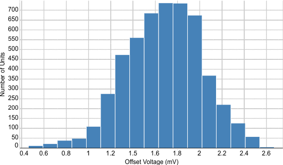
 Figure 8-25 OA Offset Voltage Sample Production Distribution
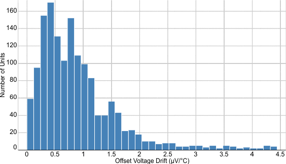
 Figure 8-26 OA Offset Voltage Drift Sample Production Distribution