ZHCSDF2E October 2014 – December 2019 MSP430FR2032 , MSP430FR2033
PRODUCTION DATA.
- 1器件概述
- 2修订历史记录
- 3Device Comparison
- 4Terminal Configuration and Functions
-
5Specifications
- 5.1 Absolute Maximum Ratings
- 5.2 ESD Ratings
- 5.3 Recommended Operating Conditions
- 5.4 Active Mode Supply Current Into VCC Excluding External Current
- 5.5 Active Mode Supply Current Per MHz
- 5.6 Low-Power Mode LPM0 Supply Currents Into VCC Excluding External Current
- 5.7 Low-Power Mode LPM3 and LPM4 Supply Currents (Into VCC) Excluding External Current
- 5.8 Low-Power Mode LPMx.5 Supply Currents (Into VCC) Excluding External Current
- 5.9 Typical Characteristics, Low-Power Mode Supply Currents
- 5.10 Typical Characteristics - Current Consumption Per Module
- 5.11 Thermal Characteristics
- 5.12
Timing and Switching Characteristics
- 5.12.1 Power Supply Sequencing
- 5.12.2 Reset Timing
- 5.12.3 Clock Specifications
- 5.12.4 Digital I/Os
- 5.12.5 Timer_A
- 5.12.6
eUSCI
- Table 5-11 eUSCI (UART Mode) Recommended Operating Conditions
- Table 5-12 eUSCI (UART Mode) Switching Characteristics
- Table 5-13 eUSCI (SPI Master Mode) Recommended Operating Conditions
- Table 5-14 eUSCI (SPI Master Mode) Switching Characteristics
- Table 5-15 eUSCI (SPI Slave Mode) Switching Characteristics
- Table 5-16 eUSCI (I2C Mode) Switching Characteristics
- 5.12.7 ADC
- 5.12.8 FRAM
- 5.12.9 Emulation and Debug
-
6Detailed Description
- 6.1 CPU
- 6.2 Operating Modes
- 6.3 Interrupt Vector Addresses
- 6.4 Bootloader (BSL)
- 6.5 JTAG Standard Interface
- 6.6 Spy-Bi-Wire Interface (SBW)
- 6.7 FRAM
- 6.8 Memory Protection
- 6.9
Peripherals
- 6.9.1 Power Management Module (PMM) and On-chip Reference Voltages
- 6.9.2 Clock System (CS) and Clock Distribution
- 6.9.3 General-Purpose Input/Output Port (I/O)
- 6.9.4 Watchdog Timer (WDT)
- 6.9.5 System Module (SYS)
- 6.9.6 Cyclic Redundancy Check (CRC)
- 6.9.7 Enhanced Universal Serial Communication Interface (eUSCI_A0, eUSCI_B0)
- 6.9.8 Timers (Timer0_A3, Timer1_A3)
- 6.9.9 Real-Time Clock (RTC) Counter
- 6.9.10 10-Bit Analog Digital Converter (ADC)
- 6.9.11 Embedded Emulation Module (EEM)
- 6.9.12
Input/Output Diagrams
- 6.9.12.1 Port P1 Input/Output With Schmitt Trigger
- 6.9.12.2 Port P2 Input/Output With Schmitt Trigger
- 6.9.12.3 Port P3 Input/Output With Schmitt Trigger
- 6.9.12.4 Port P4.0 Input/Output With Schmitt Trigger
- 6.9.12.5 Port P4.1 and P4.2 Input/Output With Schmitt Trigger
- 6.9.12.6 Port 4.3, P4.4, P4.5, P4.6, and P4.7 Input/Output With Schmitt Trigger
- 6.9.12.7 Port P5.0, P5.1, P5.2, and P5.3 Input/Output With Schmitt Trigger
- 6.9.12.8 Port P5.4, P5.5, P5.6, and P5.7 Input/Output With Schmitt Trigger
- 6.9.12.9 Port P6.0, P6.1, P6.2, and P6.3 Input/Output With Schmitt Trigger
- 6.9.12.10 Port P6.4, P6.5, P6.6, and P6.7 Input/Output With Schmitt Trigger
- 6.9.12.11 Port P7.0, P7.1, P7.2, and P7.3 Input/Output With Schmitt Trigger
- 6.9.12.12 Port P7.4, P7.5, P7.6, and P7.7 Input/Output With Schmitt Trigger
- 6.9.12.13 Port P8.0 and P8.1 Input/Output With Schmitt Trigger
- 6.9.12.14 Port P8.2 and P8.3 Input/Output With Schmitt Trigger
- 6.10 Device Descriptors (TLV)
- 6.11 Memory
- 6.12 Identification
- 7Applications, Implementation, and Layout
- 8器件和文档支持
- 9机械、封装和可订购信息
封装选项
机械数据 (封装 | 引脚)
散热焊盘机械数据 (封装 | 引脚)
订购信息
Table 5-14 eUSCI (SPI Master Mode) Switching Characteristics
over recommended ranges of supply voltage and operating free-air temperature (unless otherwise noted)(1)| PARAMETER | TEST CONDITIONS | VCC | MIN | MAX | UNIT | |
|---|---|---|---|---|---|---|
| tSTE,LEAD | STE lead time, STE active to clock | UCSTEM = 1, UCMODEx = 01 or 10 | 1 | UCxCLK cycles | ||
| tSTE,LAG | STE lag time, Last clock to STE inactive | UCSTEM = 1, UCMODEx = 01 or 10 | 1 | UCxCLK cycles | ||
| tSU,MI | SOMI input data setup time | 2 V | 45 | ns | ||
| 3 V | 35 | |||||
| tHD,MI | SOMI input data hold time | 2 V | 0 | ns | ||
| 3 V | 0 | |||||
| tVALID,MO | SIMO output data valid time(2) | UCLK edge to SIMO valid,
CL = 20 pF |
2 V | 20 | ns | |
| 3 V | 20 | |||||
| tHD,MO | SIMO output data hold time(3) | CL = 20 pF | 2 V | 0 | ns | |
| 3 V | 0 | |||||
(1) fUCxCLK = 1/2tLO/HI with tLO/HI = max(tVALID,MO(eUSCI) + tSU,SI(Slave), tSU,MI(eUSCI) + tVALID,SO(Slave))
For the slave parameters tSU,SI(Slave) and tVALID,SO(Slave), see the SPI parameters of the attached slave.
For the slave parameters tSU,SI(Slave) and tVALID,SO(Slave), see the SPI parameters of the attached slave.
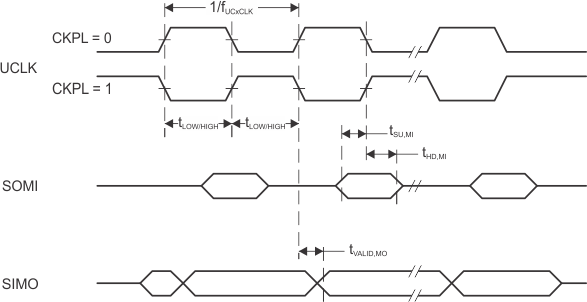
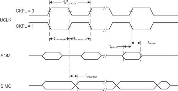
(2) Specifies the time to drive the next valid data to the SIMO output after the output changing UCLK clock edge. See the timing diagrams in Figure 5-9 and Figure 5-10.
(3) Specifies how long data on the SIMO output is valid after the output changing UCLK clock edge. Negative values indicate that the data on the SIMO output can become invalid before the output changing clock edge observed on UCLK. See the timing diagrams in Figure 5-9 and Figure 5-10.
 Figure 5-9 SPI Master Mode, CKPH = 0
  Figure 5-10 SPI Master Mode, CKPH = 1