ZHCSF32E February 2016 – December 2019 MSP430FR2310 , MSP430FR2311
PRODUCTION DATA.
- 1器件概述
- 2修订历史记录
- 3Device Comparison
- 4Terminal Configuration and Functions
-
5Specifications
- 5.1 Absolute Maximum Ratings
- 5.2 ESD Ratings
- 5.3 Recommended Operating Conditions
- 5.4 Active Mode Supply Current Into VCC Excluding External Current
- 5.5 Active Mode Supply Current Per MHz
- 5.6 Low-Power Mode LPM0 Supply Currents Into VCC Excluding External Current
- 5.7 Low-Power Mode LPM3 and LPM4 Supply Currents (Into VCC) Excluding External Current
- 5.8 Low-Power Mode LPMx.5 Supply Currents (Into VCC) Excluding External Current
- 5.9 Production Distribution of LPM Supply Currents
- 5.10 Typical Characteristics – Current Consumption Per Module
- 5.11 Thermal Resistance Characteristics
- 5.12
Timing and Switching Characteristics
- 5.12.1 Power Supply Sequencing
- 5.12.2 Reset Timing
- 5.12.3 Clock Specifications
- 5.12.4 Digital I/Os
- 5.12.5 VREF+ Built-in Reference
- 5.12.6 Timer_B
- 5.12.7
eUSCI
- Table 5-14 eUSCI (UART Mode) Clock Frequency
- Table 5-15 eUSCI (UART Mode) Switching Characteristics
- Table 5-16 eUSCI (SPI Master Mode) Clock Frequency
- Table 5-17 eUSCI (SPI Master Mode) Switching Characteristics
- Table 5-18 eUSCI (SPI Slave Mode) Switching Characteristics
- Table 5-19 eUSCI (I2C Mode) Switching Characteristics
- 5.12.8 ADC
- 5.12.9 Enhanced Comparator (eCOMP)
- 5.12.10 Smart Analog Combo (SAC)
- 5.12.11 Transimpedance Amplifier (TIA)
- 5.12.12 FRAM
- 5.12.13 Emulation and Debug
-
6Detailed Description
- 6.1 Overview
- 6.2 CPU
- 6.3 Operating Modes
- 6.4 Interrupt Vector Addresses
- 6.5 Memory Organization
- 6.6 Bootloader (BSL)
- 6.7 JTAG Standard Interface
- 6.8 Spy-Bi-Wire Interface (SBW)
- 6.9 FRAM
- 6.10 Memory Protection
- 6.11
Peripherals
- 6.11.1 Power-Management Module (PMM) and On-chip Reference Voltages
- 6.11.2 Clock System (CS) and Clock Distribution
- 6.11.3 General-Purpose Input/Output Port (I/O)
- 6.11.4 Watchdog Timer (WDT)
- 6.11.5 System Module (SYS)
- 6.11.6 Cyclic Redundancy Check (CRC)
- 6.11.7 Enhanced Universal Serial Communication Interface (eUSCI_A0, eUSCI_B0)
- 6.11.8 Timers (Timer0_B3, Timer1_B3)
- 6.11.9 Backup Memory (BAKMEM)
- 6.11.10 Real-Time Clock (RTC) Counter
- 6.11.11 10-Bit Analog-to-Digital Converter (ADC)
- 6.11.12 eCOMP0
- 6.11.13 SAC0
- 6.11.14 TIA0
- 6.11.15 eCOMP0, SAC0, TIA0, and ADC in SOC Interconnection
- 6.11.16 Embedded Emulation Module (EEM)
- 6.11.17 Peripheral File Map
- 6.12 Input/Output Diagrams
- 6.13 Device Descriptors (TLV)
- 6.14 Identification
- 7Applications, Implementation, and Layout
- 8器件和文档支持
- 9机械、封装和可订购信息
封装选项
机械数据 (封装 | 引脚)
散热焊盘机械数据 (封装 | 引脚)
- RGY|16
订购信息
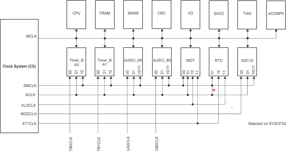
6.11.2 Clock System (CS) and Clock Distribution
The clock system includes a 32-kHz low-frequency oscillator (XT1 low frequency) or up to a 16-MHz high-frequency crystal oscillator (XT1 high frequency), an internal very low-power low-frequency oscillator (VLO), an integrated 32-kHz RC oscillator (REFO), an integrated internal digitally controlled oscillator (DCO) that can use frequency-locked loop (FLL) locking with internal or external 32-kHz reference clock, and on-chip asynchronous high-speed clock (MODOSC). The clock system is designed to target cost-effective designs with minimal external components. A fail-safe mechanism is designed for XT1. The clock system module offers the following clock signals.
- Main Clock (MCLK): system clock used by the CPU and all relevant peripherals accessed by the bus. All clock sources except MODOSC can be selected as the source with a predivider of 1, 2, 4, 8, 16, 32, 64, or 128.
- Sub-Main Clock (SMCLK): subsystem clock used by the peripheral modules. SMCLK derives from the MCLK with a predivider of 1, 2, 4, or 8. This means SMCLK is always equal to or less than MCLK.
- Auxiliary Clock (ACLK): derived from the external XT1 clock or internal REFO clock up to 40 kHz.
All peripherals may have one or several clock sources depending on specific functionality. Table 6-8 and Table 6-9 show the clock distribution used in this device.
Table 6-8 Clock Distribution
| CLOCK SOURCE SELECT BITS(1) | MCLK | SMCLK | ACLK | MODCLK | VLOCLK | EXTERNAL PIN | |
|---|---|---|---|---|---|---|---|
| Frequency Range | DC to 16 MHz | DC to 16 MHz | DC to 40 kHz | 5 MHz ±10% | 10 kHz ±50% | – | |
| CPU | N/A | Default | – | – | – | – | – |
| FRAM | N/A | Default | – | – | – | – | – |
| RAM | N/A | Default | – | – | – | – | – |
| CRC | N/A | Default | – | – | – | – | – |
| I/O | N/A | Default | – | – | – | – | |
| TB0 | TBSSEL | – | 10b | 01b | – | – | 00b (TB0CLK pin) |
| TB1 | TBSSEL | – | 10b | 01b | – | – | 00b (TB1CLK pin) |
| eUSCI_A0 | UCSSEL | – | 10b or 11b | 01b | – | – | 00b (UCA0CLK pin) |
| eUSCI_B0 | UCSSEL | – | 10b or 11b | 01b | – | – | 00b (UCB0CLK pin) |
| WDT | WDTSSEL | – | 00b | 01b | – | 10b | – |
| ADC | ADCSSEL | – | 10b or 11b | 01b | 00b | – | – |
| RTC | RTCSS | – | 01b(2) | 01b(2) | – | 11b | – |
Table 6-9 XTCLK Distribution
| OPERATION MODE | CLOCK SOURCE SELECT BITS | XTHFCLK | XTLFCLK | XTLFCLK (LPMx.5) |
|---|---|---|---|---|
| AM TO LPM0 | AM TO LPM3 | AM TO LPM3.5 | ||
| MCLK | SELMS | 10b | 10b | 10b |
| SMCLK | SELMS | 10b | 10b | 10b |
| REFO | SELREF | 0b | 0b | 0b |
| ACLK | SELA | 0b | 0b | 0b |
| RTC | RTCSS | – | 10b | 10b |
