ZHCSJG5C March 2019 – September 2021 MSP430FR2475 , MSP430FR2476
PRODUCTION DATA
- 1 特性
- 2 应用
- 3 说明
- 4 功能模块图
- 5 Revision History
- 6 Device Comparison
- 7 Terminal Configuration and Functions
-
8 Specifications
- 8.1 Absolute Maximum Ratings
- 8.2 ESD Ratings
- 8.3 Recommended Operating Conditions
- 8.4 Active Mode Supply Current Into VCC Excluding External Current
- 8.5 Active Mode Supply Current Per MHz
- 8.6 Low-Power Mode LPM0 Supply Currents Into VCC Excluding External Current
- 8.7 Low-Power Mode (LPM3, LPM4) Supply Currents (Into VCC) Excluding External Current
- 8.8 Low-Power Mode LPMx.5 Supply Currents (Into VCC) Excluding External Current
- 8.9 Typical Characteristics – Low-Power Mode Supply Currents
- 8.10 Current Consumption Per Module
- 8.11 Thermal Resistance Characteristics
- 8.12 Timing and Switching Characteristics
-
9 Detailed Description
- 9.1 Overview
- 9.2 CPU
- 9.3 Operating Modes
- 9.4 Interrupt Vector Addresses
- 9.5 Bootloader (BSL)
- 9.6 JTAG Standard Interface
- 9.7 Spy-Bi-Wire Interface (SBW)
- 9.8 FRAM
- 9.9 Memory Protection
- 9.10
Peripherals
- 9.10.1 Power-Management Module (PMM)
- 9.10.2 Clock System (CS) and Clock Distribution
- 9.10.3 General-Purpose Input/Output Port (I/O)
- 9.10.4 Watchdog Timer (WDT)
- 9.10.5 System (SYS) Module
- 9.10.6 Cyclic Redundancy Check (CRC)
- 9.10.7 Enhanced Universal Serial Communication Interface (eUSCI_A0, eUSCI_B0)
- 9.10.8 Timers (TA0, TA1, TA2, TA3 and TB0)
- 9.10.9 Hardware Multiplier (MPY)
- 9.10.10 Backup Memory (BAKMEM)
- 9.10.11 Real-Time Clock (RTC)
- 9.10.12 12-Bit Analog-to-Digital Converter (ADC)
- 9.10.13 eCOMP0
- 9.10.14 Embedded Emulation Module (EEM)
- 9.11
Input/Output Diagrams
- 9.11.1 Port P1 (P1.0 to P1.7) Input/Output With Schmitt Trigger
- 9.11.2 Port P2 (P2.0 to P2.7) Input/Output With Schmitt Trigger
- 9.11.3 Port P3 (P3.0 to P3.7) Input/Output With Schmitt Trigger
- 9.11.4 Port P4 (P4.0 to P4.7) Input/Output With Schmitt Trigger
- 9.11.5 Port P5 (P5.0 to P5.7) Input/Output With Schmitt Trigger
- 9.11.6 Port P6 (P6.0 to P6.2) Input/Output With Schmitt Trigger
- 9.12 Device Descriptors
- 9.13 Memory
- 9.14 Identification
- 10Applications, Implementation, and Layout
- 11Device and Documentation Support
- 12Mechanical, Packaging, and Orderable Information
封装选项
机械数据 (封装 | 引脚)
散热焊盘机械数据 (封装 | 引脚)
订购信息
9.10.8 Timers (TA0, TA1, TA2, TA3 and TB0)
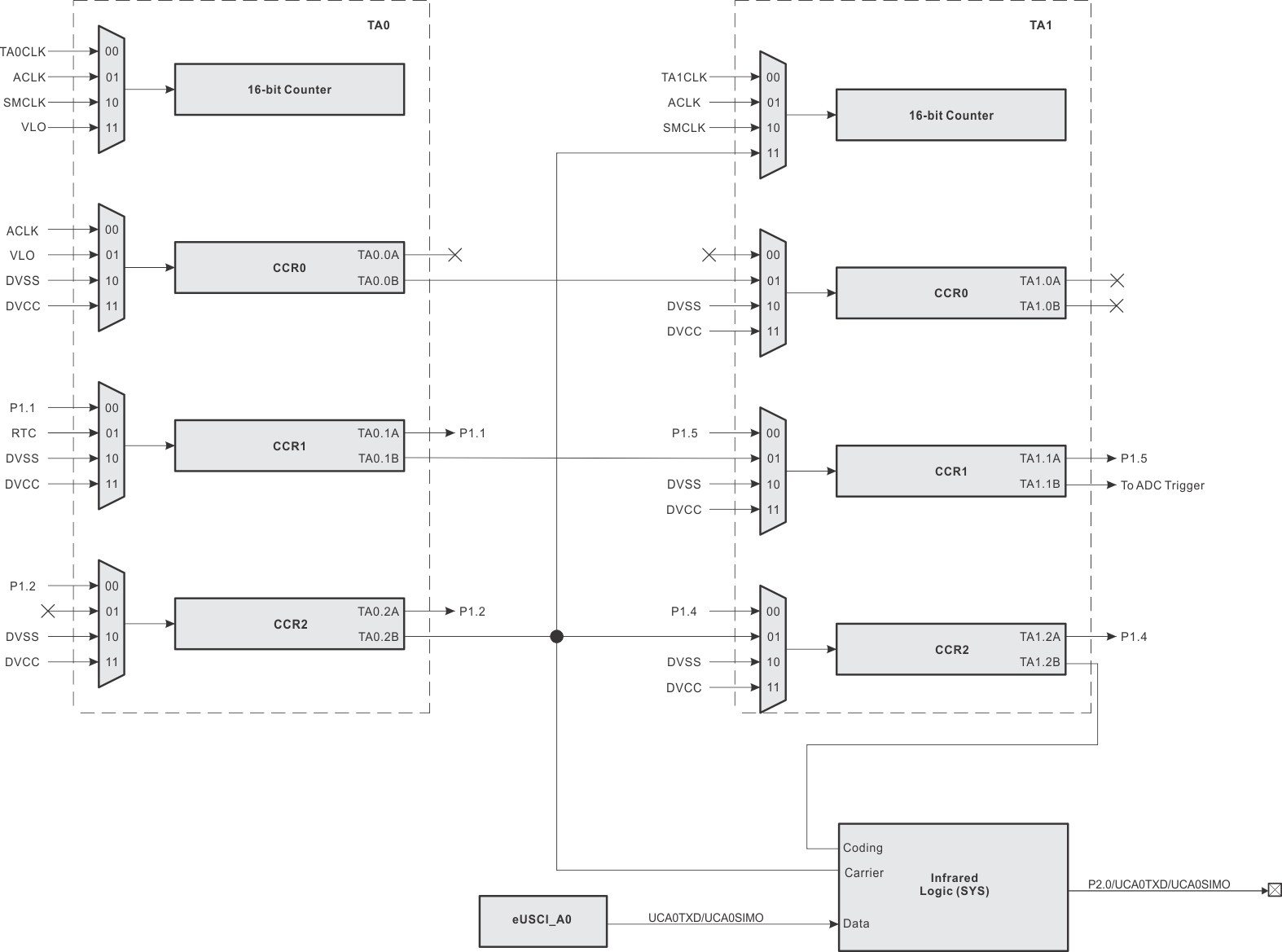
The TA0, TA1, TA2 and TA3 modules are 16-bit timers and counters with three capture/compare registers each. Each timer supports multiple captures or compares, PWM outputs, and interval timing (see Table 9-12 and Table 9-13). Each timer has extensive interrupt capabilities. Interrupts may be generated from the counter on overflow conditions and from each of the capture/compare registers. The CCR0 registers on both TA0 and TA2 are not externally connected and can only be used for hardware period timing and interrupt generation. In Up mode, they can be used to set the overflow value of the counter.
| PORT PIN | DEVICE INPUT SIGNAL | MODULE INPUT NAME | MODULE BLOCK | MODULE OUTPUT SIGNAL | DEVICE OUTPUT SIGNAL |
|---|---|---|---|---|---|
| P1.0 | TA0CLK | TACLK | Timer | N/A | |
| ACLK (internal) | ACLK | ||||
| SMCLK (internal) | SMCLK | ||||
| VLO (internal) | INCLK | ||||
| ACLK (internal) | CCI0A | CCR0 | TA0 | Not used | |
| VLO (internal) | CCI0B | Timer1_A1 CCI0B input | |||
| DVSS | GND | ||||
| DVCC | VCC | ||||
| P1.1 | TA0.1 | CCI1A | CCR1 | TA1 | TA0.1 |
| RTC (internal) | CCI1B | Timer1_A1 CCI1B input | |||
| DVSS | GND | ||||
| DVCC | VCC | ||||
| P1.2 | TA0.2 | CCI2A | CCR2 | TA2 | TA0.2 |
| N/A | CCI2B | Timer1_A1 INCLK Timer1_A1 CCI2B input, IR carrier input |
|||
| DVSS | GND | ||||
| DVCC | VCC |
| PORT PIN | DEVICE INPUT SIGNAL | MODULE INPUT NAME | MODULE BLOCK | MODULE OUTPUT SIGNAL | DEVICE OUTPUT SIGNAL |
|---|---|---|---|---|---|
| P1.6 | TA1CLK | TACLK | Timer | N/A | |
| ACLK (internal) | ACLK | ||||
| SMCLK (internal) | SMCLK | ||||
| Timer0_A3 CCR2B output (internal) | INCLK | ||||
| N/A | CCI0A | CCR0 | TA0 | Not used | |
| Timer0_A3 CCR0B output (internal) | CCI0B | Not used | |||
| DVSS | GND | ||||
| DVCC | VCC | ||||
| P1.5 | TA1.1 | CCI1A | CCR1 | TA1 | TA1.1 |
| Timer0_A3 CCR1B output (internal) | CCI1B | To ADC trigger | |||
| DVSS | GND | ||||
| DVCC | VCC | ||||
| P1.4 | TA1.2 | CCI2A | CCR2 | TA2 | TA1.2 |
| Timer0_A3 CCR2B output (internal) | CCI2B | IR coding input | |||
| DVSS | GND | ||||
| DVCC | VCC |
 Figure 9-2 TA0 and TA1 Signal Connections
| PORT PIN | DEVICE INPUT SIGNAL | MODULE INPUT NAME | MODULE BLOCK | MODULE OUTPUT SIGNAL | DEVICE OUTPUT SIGNAL |
|---|---|---|---|---|---|
| P3.4 | TA2CLK | TACLK | Timer | N/A | |
| ACLK (internal) | ACLK | ||||
| SMCLK (internal) | SMCLK | ||||
| VLO (internal) | INCLK | ||||
| P2.3 | TA2.0 | CCI0A | CCR0 | TA0 | TA2.0 |
| VLO (internal) | CCI0B | Timer3_A3 CCI0B input | |||
| DVSS | GND | ||||
| DVCC | VCC | ||||
| P3.3 | TA2.1 | CCI1A | CCR1 | TA1 | TA2.1 |
| RTC (internal) | CCI1B | Timer3_A3 CCI1B input | |||
| DVSS | GND | ||||
| DVCC | VCC | ||||
| P3.0 | TA2.2 | CCI2A | CCR2 | TA2 | TA2.2 |
| N/A | CCI2B | Timer3_A3 CCI2B input | |||
| DVSS | GND | ||||
| DVCC | VCC | ||||
| P4.2 | TA3CLK | TACLK | Timer | N/A | |
| ACLK (internal) | ACLK | ||||
| SMCLK (internal) | SMCLK | ||||
| Timer2_A3 CCR2B output (internal) | INCLK | ||||
| P4.1 | TA3.0 | CCI0A | CCR0 | TA0 | TA3.0 |
| Timer2_A3 CCR0B output (internal) | CCI0B | Timer3_B0 CCI0B input | |||
| DVSS | GND | ||||
| DVCC | VCC | ||||
| P4.0 | TA3.1 | CCI1A | CCR1 | TA1 | TA3.1 |
| Timer2_A3 CCR1B output (internal) | CCI1B | Timer3_B0 CCI1B input | |||
| DVSS | GND | ||||
| DVCC | VCC | ||||
| P3.7 | TA3.2 | CCI2A | CCR2 | TA2 | TA3.2 |
| Timer2_A3 CCR2B output (internal) | CCI2B | Timer3_B0 CCI2B input | |||
| DVSS | GND | ||||
| DVCC | VCC | ||||
| PORT PIN | DEVICE INPUT SIGNAL | MODULE INPUT NAME | MODULE BLOCK | MODULE OUTPUT SIGNAL | DEVICE OUTPUT SIGNAL |
|---|---|---|---|---|---|
| P6.1 | TB0CLK | TBCLK | Timer | N/A | |
| ACLK (internal) | ACLK | ||||
| SMCLK (internal) | SMCLK | ||||
| N/A | INCLK | ||||
| P6.2 | TB0.0 | CCI0A | CCR0 | TB0 | TB0.0 |
| Timer3_A3 CCI0B input (internal) | CCI0B | ||||
| DVSS | GND | ||||
| DVCC | VCC | ||||
| P4.7 | TB0.1 | CCI1A | CCR1 | TB1 | TB0.1 |
| Timer3_A3 CCI1B input (internal) | CCI1B | ||||
| DVSS | GND | ||||
| DVCC | VCC | ||||
| P5.0 | TB0.2 | CCI2A | CCR2 | TB2 | TB0.2 |
| Timer3_A3 CCI2B input (internal) | CCI2B | ||||
| DVSS | GND | ||||
| DVCC | VCC | ||||
| P5.1 | TB0.3 | CCI1A | CCR3 | TB3 | TB0.3 |
| N/A | CCI1B | ||||
| DVSS | GND | ||||
| DVCC | VCC | ||||
| P5.2 | TB0.4 | CCI1A | CCR4 | TB4 | TB0.4 |
| N/A | CCI1B | ||||
| DVSS | GND | ||||
| DVCC | VCC | ||||
| P4.3 | TB0.5 | CCI1A | CCR5 | TB5 | TB0.5 |
| N/A | CCI1B | ||||
| DVSS | GND | ||||
| DVCC | VCC | ||||
| P4.4 | TB0.6 | CCI1A | CCR6 | TB6 | TB0.6 |
| N/A | CCI1B | ||||
| DVSS | GND | ||||
| DVCC | VCC |
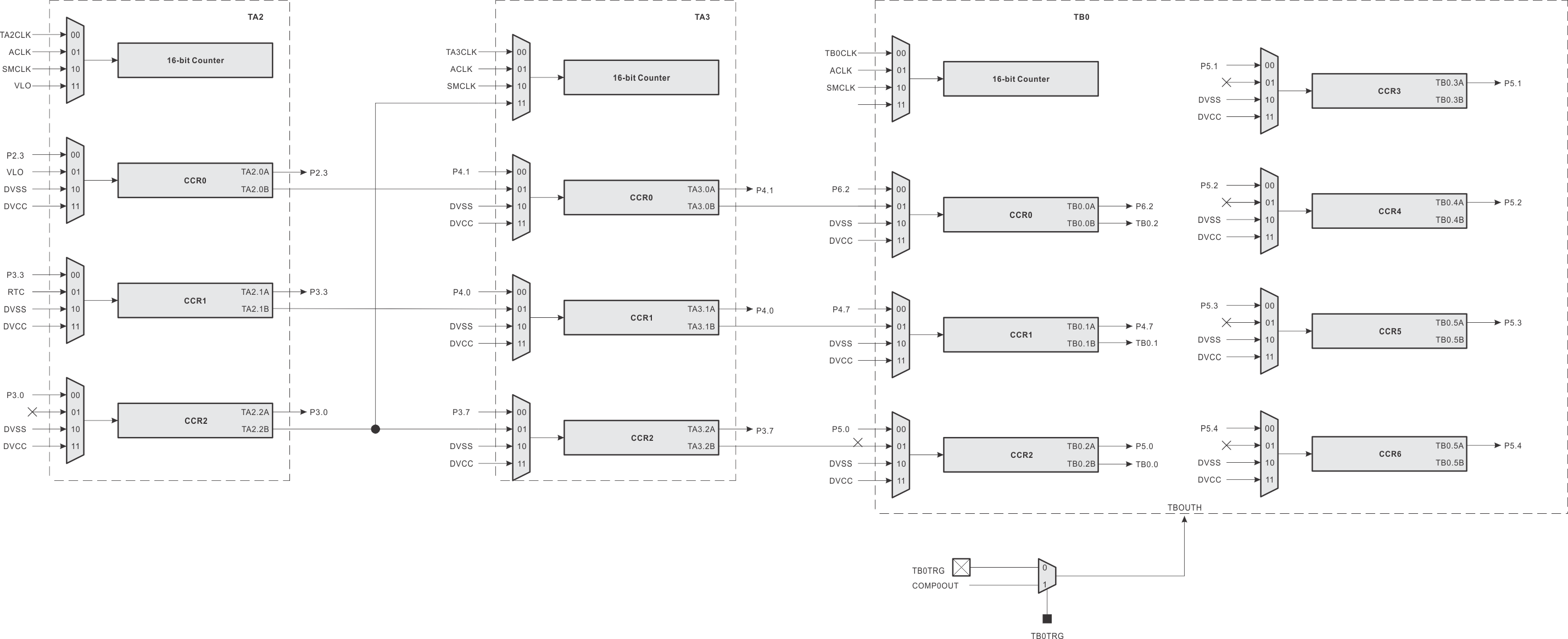
 Figure 9-3 TA2, TA3 and TB0 Signal Connections
| TA2 | PIN (PxSEL Selection) | DEVICE INPUT/OUTPUT SIGNAL |
| P3.4(1) | TA2CLK | |
| P2.3(1) | TA2.0 | |
| P3.3(1) | TA2.1 | |
| P3.0(1) | TA2.2 | |
| PIN (PxSEL Selection) | DEVICE INPUT/OUTPUT SIGNAL | |
| P5.5(2) | TA2CLK | |
| P5.6(2) | TA2.0 | |
| P5.7(2) | TA2.1 | |
| P6.0(2) | TA2.2 | |
| TA3 | PIN (PxSEL Selection) | DEVICE INPUT/OUTPUT SIGNAL |
| P4.2(1) | TA3CLK | |
| P4.1(1) | TA3.0 | |
| P4.0(1) | TA3.1 | |
| P3.7(1) | TA3.2 | |
| PIN (PxSEL Selection) | DEVICE INPUT/OUTPUT SIGNAL | |
| P5.4(2) | TA3CLK | |
| P5.3(2) | TA3.0 | |
| P4.6(2) | TA3.1 | |
| P4.5(2) | TA3.2 |
The interconnection of Timer0_A3 and Timer1_A3 can be used to modulate the eUSCI_A pin of UCA0TXD/UCA0SIMO in either ASK or FSK mode, with which a user can easily acquire a modulated infrared command for directly driving an external IR diode. The IR functions are fully controlled by SYS configuration register 1 including IREN (enable), IRPSEL (polarity select), IRMSEL (mode select), IRDSSEL (data select), and IRDATA (data) bits. For more information, see the SYS chapter in the MP430FR4xx and MP430FR2xx Family User's Guide.
The Timer_B module feature the function to put Timer_B all outputs into a high impedance state when the selected source is triggered. The source can be selected from external pin or internal of the device, it is controlled by TBxTRG in SYS. For more information, see the SYS chapter in the MP430FR4xx and MP430FR2xx Family User's Guide.
Table 9-17 lists the Timer_B high-impedance trigger source selections.
| TB0TRGSEL | TB0OUTH TRIGGER SOURCE SELECTION | Timer_B PAD OUTPUT HIGH IMPEDANCE |
|---|---|---|
| TB0TRGSEL = 0 | eCOMP0 output (internal) | P6.2, P4.7, P5.0, P5.1, P5.2, P4.3, P4.4 |
| TB0TRGSEL= 1 | P3.5 |