ZHCSJG5C March   2019  – September 2021 MSP430FR2475 , MSP430FR2476

PRODUCTION DATA  

  1. 特性
  2. 应用
  3. 说明
  4. 功能模块图
  5. Revision History
  6. Device Comparison
    1. 6.1 Related Products
  7. Terminal Configuration and Functions
    1. 7.1 Pin Diagrams
    2. 7.2 Pin Attributes
    3. 7.3 Signal Descriptions
    4. 7.4 Pin Multiplexing
    5. 7.5 Buffer Types
    6. 7.6 Connection of Unused Pins
  8. Specifications
    1. 8.1  Absolute Maximum Ratings
    2. 8.2  ESD Ratings
    3. 8.3  Recommended Operating Conditions
    4. 8.4  Active Mode Supply Current Into VCC Excluding External Current
    5. 8.5  Active Mode Supply Current Per MHz
    6. 8.6  Low-Power Mode LPM0 Supply Currents Into VCC Excluding External Current
    7. 8.7  Low-Power Mode (LPM3, LPM4) Supply Currents (Into VCC) Excluding External Current
    8. 8.8  Low-Power Mode LPMx.5 Supply Currents (Into VCC) Excluding External Current
    9. 8.9  Typical Characteristics – Low-Power Mode Supply Currents
    10. 8.10 Current Consumption Per Module
    11. 8.11 Thermal Resistance Characteristics
    12. 8.12 Timing and Switching Characteristics
      1. 8.12.1  Power Supply Sequencing
        1. 8.12.1.1 PMM, SVS and BOR
      2. 8.12.2  Reset Timing
        1. 8.12.2.1 Wake-up Times From Low-Power Modes and Reset
      3. 8.12.3  Clock Specifications
        1. 8.12.3.1 XT1 Crystal Oscillator (Low Frequency)
        2. 8.12.3.2 DCO FLL, Frequency
        3. 8.12.3.3 DCO Frequency
        4. 8.12.3.4 REFO
        5. 8.12.3.5 Internal Very-Low-Power Low-Frequency Oscillator (VLO)
        6. 8.12.3.6 Module Oscillator (MODOSC)
      4. 8.12.4  Digital I/Os
        1. 8.12.4.1 Digital Inputs
        2. 8.12.4.2 Digital Outputs
        3. 8.12.4.3 Typical Characteristics – Outputs at 3 V and 2 V
      5. 8.12.5  Internal Shared Reference
        1. 8.12.5.1 Internal Reference Characteristics
      6. 8.12.6  Timer_A and Timer_B
        1. 8.12.6.1 Timer_A
        2. 8.12.6.2 Timer_B
      7. 8.12.7  eUSCI
        1. 8.12.7.1 eUSCI (UART Mode) Clock Frequency
        2. 8.12.7.2 eUSCI (UART Mode) Timing Characteristics
        3. 8.12.7.3 eUSCI (SPI Master Mode) Clock Frequency
        4. 8.12.7.4 eUSCI (SPI Master Mode)
        5. 8.12.7.5 eUSCI (SPI Slave Mode)
        6. 8.12.7.6 eUSCI (I2C Mode)
      8. 8.12.8  ADC
        1. 8.12.8.1 ADC, Power Supply and Input Range Conditions
        2. 8.12.8.2 ADC, Timing Parameters
        3. 8.12.8.3 ADC, Linearity Parameters
      9. 8.12.9  Enhanced Comparator (eCOMP)
        1. 8.12.9.1 eCOMP0 Characteristics
      10. 8.12.10 FRAM
        1. 8.12.10.1 FRAM Characteristics
      11. 8.12.11 Debug and Emulation
        1. 8.12.11.1 JTAG, 4-Wire and Spy-Bi-Wire Interface
  9. Detailed Description
    1. 9.1  Overview
    2. 9.2  CPU
    3. 9.3  Operating Modes
    4. 9.4  Interrupt Vector Addresses
    5. 9.5  Bootloader (BSL)
    6. 9.6  JTAG Standard Interface
    7. 9.7  Spy-Bi-Wire Interface (SBW)
    8. 9.8  FRAM
    9. 9.9  Memory Protection
    10. 9.10 Peripherals
      1. 9.10.1  Power-Management Module (PMM)
      2. 9.10.2  Clock System (CS) and Clock Distribution
      3. 9.10.3  General-Purpose Input/Output Port (I/O)
      4. 9.10.4  Watchdog Timer (WDT)
      5. 9.10.5  System (SYS) Module
      6. 9.10.6  Cyclic Redundancy Check (CRC)
      7. 9.10.7  Enhanced Universal Serial Communication Interface (eUSCI_A0, eUSCI_B0)
      8. 9.10.8  Timers (TA0, TA1, TA2, TA3 and TB0)
      9. 9.10.9  Hardware Multiplier (MPY)
      10. 9.10.10 Backup Memory (BAKMEM)
      11. 9.10.11 Real-Time Clock (RTC)
      12. 9.10.12 12-Bit Analog-to-Digital Converter (ADC)
      13. 9.10.13 eCOMP0
      14. 9.10.14 Embedded Emulation Module (EEM)
    11. 9.11 Input/Output Diagrams
      1. 9.11.1 Port P1 (P1.0 to P1.7) Input/Output With Schmitt Trigger
      2. 9.11.2 Port P2 (P2.0 to P2.7) Input/Output With Schmitt Trigger
      3. 9.11.3 Port P3 (P3.0 to P3.7) Input/Output With Schmitt Trigger
      4. 9.11.4 Port P4 (P4.0 to P4.7) Input/Output With Schmitt Trigger
      5. 9.11.5 Port P5 (P5.0 to P5.7) Input/Output With Schmitt Trigger
      6. 9.11.6 Port P6 (P6.0 to P6.2) Input/Output With Schmitt Trigger
    12. 9.12 Device Descriptors
    13. 9.13 Memory
      1. 9.13.1 Memory Organization
      2. 9.13.2 Peripheral File Map
    14. 9.14 Identification
      1. 9.14.1 Revision Identification
      2. 9.14.2 Device Identification
      3. 9.14.3 JTAG Identification
  10. 10Applications, Implementation, and Layout
    1. 10.1 Device Connection and Layout Fundamentals
      1. 10.1.1 Power Supply Decoupling and Bulk Capacitors
      2. 10.1.2 External Oscillator
      3. 10.1.3 JTAG
      4. 10.1.4 Reset
      5. 10.1.5 Unused Pins
      6. 10.1.6 General Layout Recommendations
      7. 10.1.7 Do's and Don'ts
    2. 10.2 Peripheral- and Interface-Specific Design Information
      1. 10.2.1 ADC Peripheral
        1. 10.2.1.1 Partial Schematic
        2. 10.2.1.2 Design Requirements
        3. 10.2.1.3 Layout Guidelines
  11. 11Device and Documentation Support
    1. 11.1 Getting Started and Next Steps
    2. 11.2 Device Nomenclature
    3. 11.3 Tools and Software
    4. 11.4 Documentation Support
    5. 11.5 支持资源
    6. 11.6 Trademarks
    7. 11.7 Electrostatic Discharge Caution
    8. 11.8 Export Control Notice
    9. 11.9 术语表
  12. 12Mechanical, Packaging, and Orderable Information

封装选项

机械数据 (封装 | 引脚)
散热焊盘机械数据 (封装 | 引脚)
订购信息

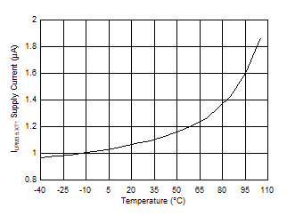
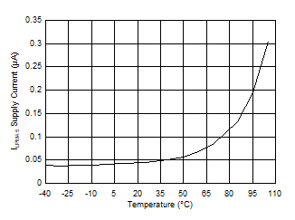
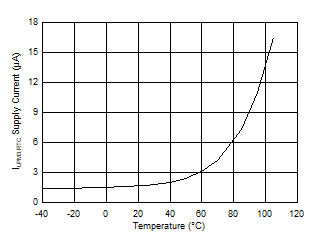
Typical Characteristics – Low-Power Mode Supply Currents

GUID-A9F68705-DA21-4CAF-AD9E-C77E63B3DF60-low.gif
VCC = 3 VRTC enabledSVS disabled
Figure 8-1 LPM3 Supply Current vs Temperature
GUID-A7FB2EC2-4CAF-4DEB-B85B-2993E7AECA2C-low.gif
VCC = 3 VXT1 enabledSVS enabled
Figure 8-3 LPM3.5 Supply Current vs Temperature
GUID-F3C81D62-ED81-4460-86F3-F07DC7E60B06-low.gif
VCC = 2 VRTC enabledSVS disabled
Figure 8-2 LPM3 Supply Current vs Temperature
GUID-66782A97-2636-4B86-83B1-B7EA29134951-low.gif
VCC = 3 VSVS disabled
Figure 8-4 LPM4.5 Supply Current vs Temperature