ZHCSET6E November   2015  – December 2019 MSP430FR2532 , MSP430FR2533 , MSP430FR2632 , MSP430FR2633

PRODUCTION DATA.  

  1. 1器件概述
    1. 1.1 特性
    2. 1.2 应用
    3. 1.3 说明
    4. 1.4 功能框图
  2. 2修订历史记录
  3. 3Device Comparison
    1. 3.1 Related Products
  4. 4Terminal Configuration and Functions
    1. 4.1 Pin Diagrams
    2. 4.2 Pin Attributes
    3. 4.3 Signal Descriptions
    4. 4.4 Pin Multiplexing
    5. 4.5 Buffer Types
    6. 4.6 Connection of Unused Pins
  5. 5Specifications
    1. 5.1       Absolute Maximum Ratings
    2. 5.2       ESD Ratings
    3. 5.3       Recommended Operating Conditions
    4. 5.4       Active Mode Supply Current Into VCC Excluding External Current
    5. 5.5       Active Mode Supply Current Per MHz
    6. 5.6       Low-Power Mode LPM0 Supply Currents Into VCC Excluding External Current
    7. 5.7       Low-Power Mode (LPM3 and LPM4) Supply Currents (Into VCC) Excluding External Current
    8. 5.8       Low-Power Mode LPMx.5 Supply Currents (Into VCC) Excluding External Current
    9. 5.9       Typical Characteristics - Low-Power Mode Supply Currents
    10. Table 5-1 Typical Characteristics – Current Consumption Per Module
    11. 5.10      Thermal Resistance Characteristics
    12. 5.11      Timing and Switching Characteristics
      1. 5.11.1  Power Supply Sequencing
        1. Table 5-2 PMM, SVS and BOR
      2. 5.11.2  Reset Timing
        1. Table 5-3 Wake-up Times From Low-Power Modes and Reset
      3. 5.11.3  Clock Specifications
        1. Table 5-4 XT1 Crystal Oscillator (Low Frequency)
        2. Table 5-5 DCO FLL, Frequency
        3. Table 5-6 DCO Frequency
        4. Table 5-7 REFO
        5. Table 5-8 Internal Very-Low-Power Low-Frequency Oscillator (VLO)
        6. Table 5-9 Module Oscillator (MODOSC)
      4. 5.11.4  Digital I/Os
        1. Table 5-10 Digital Inputs
        2. Table 5-11 Digital Outputs
        3. 5.11.4.1   Typical Characteristics – Outputs at 3 V and 2 V
      5. 5.11.5  VREF+ Built-in Reference
        1. Table 5-12 VREF+
      6. 5.11.6  Timer_A
        1. Table 5-13 Timer_A
      7. 5.11.7  eUSCI
        1. Table 5-14 eUSCI (UART Mode) Clock Frequency
        2. Table 5-15 eUSCI (UART Mode)
        3. Table 5-16 eUSCI (SPI Master Mode) Clock Frequency
        4. Table 5-17 eUSCI (SPI Master Mode)
        5. Table 5-18 eUSCI (SPI Slave Mode)
        6. Table 5-19 eUSCI (I2C Mode)
      8. 5.11.8  ADC
        1. Table 5-20 ADC, Power Supply and Input Range Conditions
        2. Table 5-21 ADC, 10-Bit Timing Parameters
        3. Table 5-22 ADC, 10-Bit Linearity Parameters
      9. 5.11.9  CapTIvate
        1. Table 5-23 CapTIvate Electrical Characteristics
        2. Table 5-24 CapTIvate Signal-to-Noise Ratio Characteristics
      10. 5.11.10 FRAM
        1. Table 5-25 FRAM
      11. 5.11.11 Debug and Emulation
        1. Table 5-26 JTAG, Spy-Bi-Wire Interface
        2. Table 5-27 JTAG, 4-Wire Interface
  6. 6Detailed Description
    1. 6.1  Overview
    2. 6.2  CPU
    3. 6.3  Operating Modes
    4. 6.4  Interrupt Vector Addresses
    5. 6.5  Bootloader (BSL)
    6. 6.6  JTAG Standard Interface
    7. 6.7  Spy-Bi-Wire Interface (SBW)
    8. 6.8  FRAM
    9. 6.9  Memory Protection
    10. 6.10 Peripherals
      1. 6.10.1  Power-Management Module (PMM)
      2. 6.10.2  Clock System (CS) and Clock Distribution
      3. 6.10.3  General-Purpose Input/Output Port (I/O)
      4. 6.10.4  Watchdog Timer (WDT)
      5. 6.10.5  System (SYS) Module
      6. 6.10.6  Cyclic Redundancy Check (CRC)
      7. 6.10.7  Enhanced Universal Serial Communication Interface (eUSCI_A0, eUSCI_B0)
      8. 6.10.8  Timers (Timer0_A3, Timer1_A3, Timer2_A2 and Timer3_A2)
      9. 6.10.9  Hardware Multiplier (MPY)
      10. 6.10.10 Backup Memory (BAKMEM)
      11. 6.10.11 Real-Time Clock (RTC)
      12. 6.10.12 10-Bit Analog-to-Digital Converter (ADC)
      13. 6.10.13 CapTIvate Technology
      14. 6.10.14 Embedded Emulation Module (EEM)
    11. 6.11 Input/Output Diagrams
      1. 6.11.1 Port P1 Input/Output With Schmitt Trigger
      2. 6.11.2 Port P2 (P2.0 to P2.2) Input/Output With Schmitt Trigger
      3. 6.11.3 Port P2 (P2.3 to P2.7) Input/Output With Schmitt Trigger
      4. 6.11.4 Port P3 (P3.0 to P3.2) Input/Output With Schmitt Trigger
    12. 6.12 Device Descriptors
    13. 6.13 Memory
      1. 6.13.1 Memory Organization
      2. 6.13.2 Peripheral File Map
    14. 6.14 Identification
      1. 6.14.1 Revision Identification
      2. 6.14.2 Device Identification
      3. 6.14.3 JTAG Identification
  7. 7Applications, Implementation, and Layout
    1. 7.1 Device Connection and Layout Fundamentals
      1. 7.1.1 Power Supply Decoupling and Bulk Capacitors
      2. 7.1.2 External Oscillator
      3. 7.1.3 JTAG
      4. 7.1.4 Reset
      5. 7.1.5 Unused Pins
      6. 7.1.6 General Layout Recommendations
      7. 7.1.7 Do's and Don'ts
    2. 7.2 Peripheral- and Interface-Specific Design Information
      1. 7.2.1 ADC Peripheral
        1. 7.2.1.1 Partial Schematic
        2. 7.2.1.2 Design Requirements
        3. 7.2.1.3 Layout Guidelines
      2. 7.2.2 CapTIvate Peripheral
        1. 7.2.2.1 Device Connection and Layout Fundamentals
        2. 7.2.2.2 Measurements
          1. 7.2.2.2.1 SNR
          2. 7.2.2.2.2 Sensitivity
          3. 7.2.2.2.3 Power
    3. 7.3 CapTIvate Technology Evaluation
  8. 8器件和文档支持
    1. 8.1  入门和后续步骤
    2. 8.2  器件命名规则
    3. 8.3  工具和软件
    4. 8.4  文档支持
    5. 8.5  相关链接
    6. 8.6  社区资源
    7. 8.7  商标
    8. 8.8  静电放电警告
    9. 8.9  Export Control Notice
    10. 8.10 Glossary
  9. 9机械、封装和可订购信息

封装选项

机械数据 (封装 | 引脚)
散热焊盘机械数据 (封装 | 引脚)
订购信息

Pin Diagrams

Figure 4-1 shows the pinout for the 32-pin RHB package.
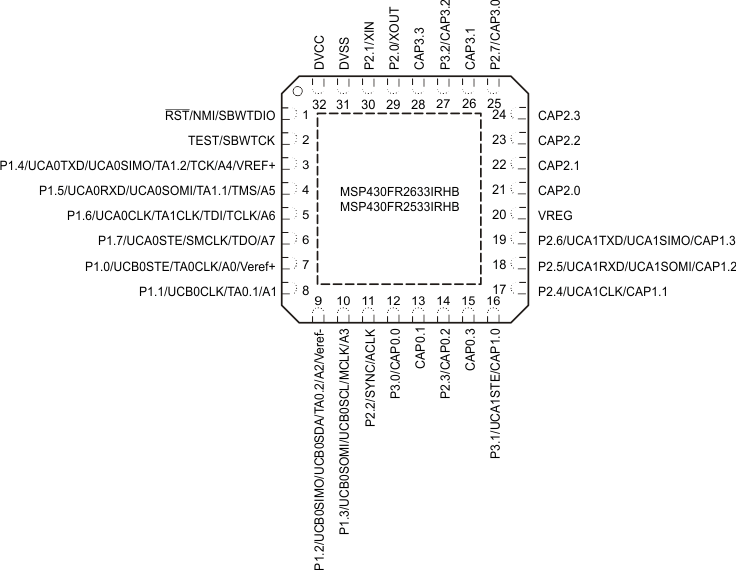
MSP430FR2633 MSP430FR2632 MSP430FR2533 MSP430FR2532 SLAS942_PINOUT_QFN32.gifFigure 4-1 32-Pin RHB Package (Top View)

Figure 4-2 shows the pinout for the 32-pin DA package.

MSP430FR2633 MSP430FR2632 MSP430FR2533 MSP430FR2532 SLAS942__PINOUT_TSSOP32.gifFigure 4-2 32-Pin DA Package (Top View)

Figure 4-3 shows the pinout for the 24-pin RGE package.
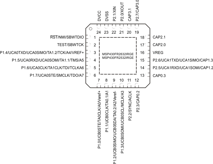
MSP430FR2633 MSP430FR2632 MSP430FR2533 MSP430FR2532 SLAS942_PINOUT_QFN24.gifFigure 4-3 24-Pin RGE Package (Top View)

Figure 4-4 shows the top view of the YQW package, and Figure 4-5 shows the bottom (ball-side) view.

MSP430FR2633 MSP430FR2632 MSP430FR2533 MSP430FR2532 SLAS942__PINOUT_DSBGA_TOPCP_YQW.gifFigure 4-4 24-Pin YQW Package (Top View)
MSP430FR2633 MSP430FR2632 MSP430FR2533 MSP430FR2532 SLAS942__PINOUT_DSBGA_BTCP_YQW.gifFigure 4-5 24-Pin YQW Package (Bottom View)