ZHCSDF6F October 2014 – December 2021 MSP430FR4131 , MSP430FR4132 , MSP430FR4133
PRODUCTION DATA
- 1 特性
- 2 应用
- 3 说明
- 4 功能方框图
- 5 Revision History
- 6 Device Comparison
- 7 Terminal Configuration and Functions
-
8 Specifications
- 8.1 Absolute Maximum Ratings
- 8.2 ESD Ratings
- 8.3 Recommended Operating Conditions
- 8.4 Active Mode Supply Current Into VCC Excluding External Current
- 8.5 Active Mode Supply Current Per MHz
- 8.6 Low-Power Mode LPM0 Supply Currents Into VCC Excluding External Current
- 8.7 Low-Power Mode LPM3, LPM4 Supply Currents (Into VCC) Excluding External Current
- 8.8 Low-Power Mode LPMx.5 Supply Currents (Into VCC) Excluding External Current
- 8.9 Typical Characteristics, Low-Power Mode Supply Currents
- 8.10 Current Consumption Per Module
- 8.11 Thermal Characteristics
- 8.12
Timing and Switching Characteristics
- 8.12.1 Power Supply Sequencing
- 8.12.2 Reset Timing
- 8.12.3 Clock Specifications
- 8.12.4 Digital I/Os
- 8.12.5 Timer_A
- 8.12.6
eUSCI
- 8.12.6.1 eUSCI (UART Mode) Operating Frequency
- 8.12.6.2 eUSCI (UART Mode) Switching Characteristics
- 8.12.6.3 eUSCI (SPI Master Mode) Operating Frequency
- 8.12.6.4 eUSCI (SPI Master Mode) Switching Characteristics
- 8.12.6.5 eUSCI (SPI Slave Mode) Switching Characteristics
- 8.12.6.6 eUSCI (I2C Mode) Switching Characteristics
- 8.12.7 ADC
- 8.12.8 LCD Controller
- 8.12.9 FRAM
- 8.12.10 Emulation and Debug
-
9 Detailed Description
- 9.1 CPU
- 9.2 Operating Modes
- 9.3 Interrupt Vector Addresses
- 9.4 Bootloader (BSL)
- 9.5 JTAG Standard Interface
- 9.6 Spy-Bi-Wire Interface (SBW)
- 9.7 FRAM
- 9.8 Memory Protection
- 9.9
Peripherals
- 9.9.1 Power Management Module (PMM) and On-Chip Reference Voltages
- 9.9.2 Clock System (CS) and Clock Distribution
- 9.9.3 General-Purpose Input/Output Port (I/O)
- 9.9.4 Watchdog Timer (WDT)
- 9.9.5 System Module (SYS)
- 9.9.6 Cyclic Redundancy Check (CRC)
- 9.9.7 Enhanced Universal Serial Communication Interface (eUSCI_A0, eUSCI_B0)
- 9.9.8 Timers (Timer0_A3, Timer1_A3)
- 9.9.9 Real-Time Clock (RTC) Counter
- 9.9.10 10-Bit Analog Digital Converter (ADC)
- 9.9.11 Liquid Crystal Display (LCD)
- 9.9.12 Embedded Emulation Module (EEM)
- 9.9.13
Input/Output Schematics
- 9.9.13.1 Port P1 Input/Output With Schmitt Trigger
- 9.9.13.2 Port P2 Input/Output With Schmitt Trigger
- 9.9.13.3 Port P3 Input/Output With Schmitt Trigger
- 9.9.13.4 Port P4.0 Input/Output With Schmitt Trigger
- 9.9.13.5 Port P4.1 and P4.2 Input/Output With Schmitt Trigger
- 9.9.13.6 Port 4.3, P4.4, P4.5, P4.6, and P4.7 Input/Output With Schmitt Trigger
- 9.9.13.7 Port P5.0, P5.1, P5.2, and P5.3 Input/Output With Schmitt Trigger
- 9.9.13.8 Port P5.4, P5.5, P5.6, and P5.7 Input/Output With Schmitt Trigger
- 9.9.13.9 Port P6 Input/Output With Schmitt Trigger
- 9.9.13.10 Port P7 Input/Output With Schmitt Trigger
- 9.9.13.11 Port P8.0 and P8.1 Input/Output With Schmitt Trigger
- 9.9.13.12 Port P8.2 and P8.3 Input/Output With Schmitt Trigger
- 9.10 Device Descriptors (TLV)
- 9.11 Memory
- 9.12 Identification
- 10Applications, Implementation, and Layout
- 11Device and Documentation Support
- 12Mechanical, Packaging, and Orderable Information
封装选项
机械数据 (封装 | 引脚)
散热焊盘机械数据 (封装 | 引脚)
订购信息
9.9.2 Clock System (CS) and Clock Distribution
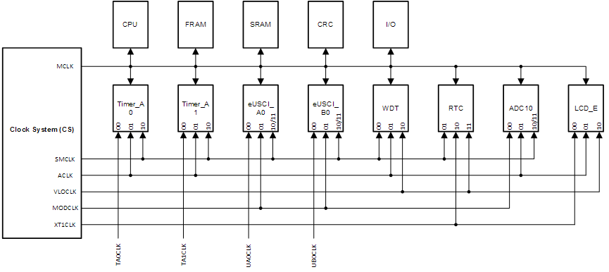
The clock system includes a 32-kHz crystal oscillator (XT1), an internal very low-power low-frequency oscillator (VLO), an integrated 32-kHz RC oscillator (REFO), an integrated internal digitally controlled oscillator (DCO) that may use frequency-locked loop (FLL) locking with internal or external 32-kHz reference clock, and on-chip asynchronous high-speed clock (MODCLK). The clock system is designed to target cost-effective designs with minimal external components. A fail-safe mechanism is designed for XT1. The clock system module offers the following clock signals.
- Main Clock (MCLK): the system clock used by the CPU and all relevant peripherals accessed by the bus. All clock sources except MODCLK can be selected as the source with a predivider of 1, 2, 4, 8, 16, 32, 64, or 128.
- Sub-Main Clock (SMCLK): the subsystem clock used by the peripheral modules. SMCLK derives from the MCLK with a predivider of 1, 2, 4, or 8. This means SMCLK is always equal to or less than MCLK.
- Auxiliary Clock (ACLK): this clock is derived from the external XT1 clock or internal REFO clock up to 40 kHz.
All peripherals may have one or several clock sources depending on specific functionality. Table 9-6 shows the clock distribution used in this device.
| CLOCK SOURCE SELECT BITS | MCLK | SMCLK | ACLK | MODCLK | XT1CLK(1) | VLOCLK | EXTERNAL PIN | |
|---|---|---|---|---|---|---|---|---|
| Frequency Range | DC to 16 MHz | DC to 16 MHz | DC to 40 kHz | 5 MHz ±10% | DC to 40 kHz | 10 kHz ±50% | ||
| CPU | N/A | Default | ||||||
| FRAM | N/A | Default | ||||||
| RAM | N/A | Default | ||||||
| CRC | N/A | Default | ||||||
| I/O | N/A | Default | ||||||
| TA0 | TASSEL | 10b | 01b | 00b (TA0CLK pin) | ||||
| TA1 | TASSEL | 10b | 01b | 00b (TA1CLK pin) | ||||
| eUSCI_A0 | UCSSELx | 10b or 11b | 01b | 00b (UCA0CLK pin) | ||||
| eUSCI_B0 | UCSSELx | 10b or 11b | 01b | 00b (UCB0CLK pin) | ||||
| WDT | WDTSSEL | 00b | 01b | 10b | ||||
| ADC | ADCSSEL | 10b or 11b | 01b | 00b | ||||
| LCD | LCDSSEL | 01b | 00b | 10b | ||||
| RTC | RTCSS | 01b | 10b | 11b |
 Figure 9-1 Clock Distribution Block Diagram