ZHCSCG3C May 2014 – December 2017 MSP430FR5720 , MSP430FR5721 , MSP430FR5722 , MSP430FR5723 , MSP430FR5724 , MSP430FR5725 , MSP430FR5726 , MSP430FR5727 , MSP430FR5728 , MSP430FR5729
PRODUCTION DATA.
- 1器件概述
- 2修订历史记录
- 3Device Comparison
-
4Terminal Configuration and Functions
- 4.1 Pin Diagram – RHA Package – MSP430FR5721, MSP430FR5723, MSP430FR5725, MSP430FR5727, MSP430FR5729
- 4.2 Pin Diagram – DA Package – MSP430FR5721, MSP430FR5723, MSP430FR5725, MSP430FR5727, MSP430FR5729
- 4.3 Pin Diagram – RGE Package – MSP430FR5720, MSP430FR5722, MSP430FR5724, MSP430FR5726, MSP430FR5728
- 4.4 Pin Diagram – PW Package – MSP430FR5720, MSP430FR5722, MSP430FR5724, MSP430FR5726, MSP430FR5728
- 4.5 Signal Descriptions
-
5Specifications
- 5.1 Absolute Maximum Ratings
- 5.2 ESD Ratings
- 5.3 Recommended Operating Conditions
- 5.4 Active Mode Supply Current Into VCC Excluding External Current
- 5.5 Low-Power Mode Supply Currents (Into VCC) Excluding External Current
- 5.6 Thermal Resistance Characteristics
- 5.7 Schmitt-Trigger Inputs – General-Purpose I/O (P1.0 to P1.7, P2.0 to P2.7, P3.0 to P3.7, P4.0 to P4.1, PJ.0 to PJ.5, RST/NMI)
- 5.8 Inputs – Ports P1 and P2 (P1.0 to P1.7, P2.0 to P2.7)
- 5.9 Leakage Current – General-Purpose I/O (P1.0 to P1.7, P2.0 to P2.7, P3.0 to P3.7, P4.0 to P4.1, PJ.0 to PJ.5, RST/NMI)
- 5.10 Outputs – General-Purpose I/O (P1.0 to P1.7, P2.0 to P2.7, P3.0 to P3.7, P4.0 to P4.1, PJ.0 to PJ.5)
- 5.11 Output Frequency – General-Purpose I/O (P1.0 to P1.7, P2.0 to P2.7, P3.0 to P3.7, P4.0 to P4.1, PJ.0 to PJ.5)
- 5.12 Typical Characteristics – Outputs
- 5.13 Crystal Oscillator, XT1, Low-Frequency (LF) Mode
- 5.14 Crystal Oscillator, XT1, High-Frequency (HF) Mode
- 5.15 Internal Very-Low-Power Low-Frequency Oscillator (VLO)
- 5.16 DCO Frequencies
- 5.17 MODOSC
- 5.18 PMM, Core Voltage
- 5.19 PMM, SVS, BOR
- 5.20 Wake-up Times From Low-Power Modes
- 5.21 Timer_A
- 5.22 Timer_B
- 5.23 eUSCI (UART Mode) Clock Frequency
- 5.24 eUSCI (UART Mode)
- 5.25 eUSCI (SPI Master Mode) Clock Frequency
- 5.26 eUSCI (SPI Master Mode)
- 5.27 eUSCI (SPI Slave Mode)
- 5.28 eUSCI (I2C Mode)
- 5.29 10-Bit ADC, Power Supply and Input Range Conditions
- 5.30 10-Bit ADC, Timing Parameters
- 5.31 10-Bit ADC, Linearity Parameters
- 5.32 REF, External Reference
- 5.33 REF, Built-In Reference
- 5.34 REF, Temperature Sensor and Built-In VMID
- 5.35 Comparator_D
- 5.36 FRAM
- 5.37 JTAG and Spy-Bi-Wire Interface
-
6Detailed Description
- 6.1 Functional Block Diagrams
- 6.2 CPU
- 6.3 Operating Modes
- 6.4 Interrupt Vector Addresses
- 6.5 Memory Organization
- 6.6 Bootloader (BSL)
- 6.7 JTAG Operation
- 6.8 FRAM
- 6.9 Memory Protection Unit (MPU)
- 6.10
Peripherals
- 6.10.1 Digital I/O
- 6.10.2 Oscillator and Clock System (CS)
- 6.10.3 Power-Management Module (PMM)
- 6.10.4 Hardware Multiplier (MPY)
- 6.10.5 Real-Time Clock (RTC_B)
- 6.10.6 Watchdog Timer (WDT_A)
- 6.10.7 System Module (SYS)
- 6.10.8 DMA Controller
- 6.10.9 Enhanced Universal Serial Communication Interface (eUSCI)
- 6.10.10 TA0, TA1
- 6.10.11 TB0, TB1, TB2
- 6.10.12 ADC10_B
- 6.10.13 Comparator_D
- 6.10.14 CRC16
- 6.10.15 Shared Reference (REF)
- 6.10.16 Embedded Emulation Module (EEM)
- 6.10.17 Peripheral File Map
- 6.11
Input/Output Diagrams
- 6.11.1 Port P1 (P1.0 to P1.2) Input/Output With Schmitt Trigger
- 6.11.2 Port P1 (P1.3 to P1.5) Input/Output With Schmitt Trigger
- 6.11.3 Port P1 (P1.6 and P1.7) Input/Output With Schmitt Trigger
- 6.11.4 Port P2 (P2.0 to P2.2) Input/Output With Schmitt Trigger
- 6.11.5 Port P2 (P2.3 and P2.4) Input/Output With Schmitt Trigger
- 6.11.6 Port P2 (P2.5 and P2.6) Input/Output With Schmitt Trigger
- 6.11.7 Port P2 (P2.7) Input/Output With Schmitt Trigger
- 6.11.8 Port P3 (P3.0 to P3.3) Input/Output With Schmitt Trigger
- 6.11.9 Port P3 (P3.4 to P3.6) Input/Output With Schmitt Trigger
- 6.11.10 Port Port P3 (P3.7) Input/Output With Schmitt Trigger
- 6.11.11 Port Port P4 (P4.0) Input/Output With Schmitt Trigger
- 6.11.12 Port Port P4 (P4.1) Input/Output With Schmitt Trigger
- 6.11.13 Port Port PJ (PJ.0 to PJ.3) JTAG Pins TDO, TMS, TCK, TDI/TCLK, Input/Output With Schmitt Trigger or Output
- 6.11.14 Port Port PJ (PJ.4 and PJ.5) Input/Output With Schmitt Trigger
- 6.12 Device Descriptors (TLV)
- 7器件和文档支持
- 8机械、封装和可订购信息
封装选项
机械数据 (封装 | 引脚)
散热焊盘机械数据 (封装 | 引脚)
- RGE|24
订购信息
5.34 REF, Temperature Sensor and Built-In VMID
over recommended ranges of supply voltage and operating free-air temperature (unless otherwise noted)| PARAMETER | TEST CONDITIONS | VCC | MIN | TYP | MAX | UNIT | |
|---|---|---|---|---|---|---|---|
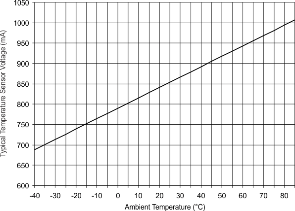
| VSENSOR | See (1) | ADC10ON = 1, INCH = 0Ah, TA = 0°C |
2 V, 3 V | 790 | mV | ||
| TCSENSOR | ADC10ON = 1, INCH = 0Ah | 2 V, 3 V | 2.55 | mV/°C | |||
| tSENSOR(sample) | Sample time required if channel 10 is selected (2) | ADC10ON = 1, INCH = 0Ah, Error of conversion result ≤ 1 LSB |
2 V | 30 | µs | ||
| 3 V | 30 | ||||||
| VMID | AVCC divider at channel 11 | ADC10ON = 1, INCH = 0Bh, VMID is ~0.5 × VAVCC |
2 V | 0.97 | 1.0 | 1.03 | V |
| 3 V | 1.46 | 1.5 | 1.54 | ||||
| tVMID(sample) | Sample time required if channel 11 is selected (3) | ADC10ON = 1, INCH = 0Bh, Error of conversion result ≤ 1 LSB |
2 V, 3 V | 1000 | ns | ||
(1) The temperature sensor offset can vary significantly. A single-point calibration is recommended to minimize the offset error of the built-in temperature sensor.
(2) The typical equivalent impedance of the sensor is 51 kΩ. The sample time required includes the sensor-on time tSENSOR(on).
(3) The on-time tVMID(on) is included in the sampling time tVMID(sample); no additional on time is needed.
 Figure 5-11 Typical Temperature Sensor Voltage