ZHCSGO9C June 2017 – September 2018 MSP430FR6035 , MSP430FR6037 , MSP430FR60371 , MSP430FR6045 , MSP430FR6047 , MSP430FR60471
PRODUCTION DATA.
- 1器件概述
- 2修订历史记录
- 3Device Comparison
- 4Terminal Configuration and Functions
-
5Specifications
- 5.1 Absolute Maximum Ratings
- 5.2 ESD Ratings
- 5.3 Recommended Operating Conditions
- 5.4 Active Mode Supply Current Into VCC Excluding External Current
- 5.5 Typical Characteristics, Active Mode Supply Currents
- 5.6 Low-Power Mode (LPM0, LPM1) Supply Currents Into VCC Excluding External Current
- 5.7 Low-Power Mode (LPM2, LPM3, LPM4) Supply Currents (Into VCC) Excluding External Current
- 5.8 Low-Power Mode With LCD Supply Currents (Into VCC) Excluding External Current
- 5.9 Low-Power Mode (LPMx.5) Supply Currents (Into VCC) Excluding External Current
- 5.10 Typical Characteristics, Low-Power Mode Supply Currents
- 5.11 Typical Characteristics, Current Consumption per Module
- 5.12 Thermal Resistance Characteristics for 100-Pin LQFP (PZ) Package
- 5.13
Timing and Switching Characteristics
- 5.13.1 Power Supply Sequencing
- 5.13.2 Reset Timing
- 5.13.3 Clock Specifications
- 5.13.4 Wake-up Characteristics
- 5.13.5 Digital I/Os
- 5.13.6 LEA
- 5.13.7 Timer_A and Timer_B
- 5.13.8
eUSCI
- Table 5-16 eUSCI (UART Mode) Clock Frequency
- Table 5-17 eUSCI (UART Mode) Switching Characteristics
- Table 5-18 eUSCI (SPI Master Mode) Clock Frequency
- Table 5-19 eUSCI (SPI Master Mode) Switching Characteristics
- Table 5-20 eUSCI (SPI Slave Mode) Switching Characteristics
- Table 5-21 eUSCI (I2C Mode) Switching Characteristics
- 5.13.9 Segment LCD Controller
- 5.13.10
ADC12_B
- Table 5-24 12-Bit ADC, Power Supply and Input Range Conditions
- Table 5-25 12-Bit ADC, Timing Parameters
- Table 5-26 12-Bit ADC, Linearity Parameters
- Table 5-27 12-Bit ADC, Dynamic Performance With External Reference
- Table 5-28 12-Bit ADC, Dynamic Performance With Internal Reference
- Table 5-29 12-Bit ADC, Temperature Sensor and Built-In V1/2
- Table 5-30 12-Bit ADC, External Reference
- 5.13.11 Reference
- 5.13.12 Comparator
- 5.13.13 FRAM
- 5.13.14 USS
- 5.13.15 Emulation and Debug
-
6Detailed Description
- 6.1 Overview
- 6.2 CPU
- 6.3 Ultrasonic Sensing Solution (USS) Module
- 6.4 Low-Energy Accelerator (LEA) for Signal Processing
- 6.5 Operating Modes
- 6.6 Interrupt Vector Table and Signatures
- 6.7 Bootloader (BSL)
- 6.8 JTAG Operation
- 6.9 FRAM Controller A (FRCTL_A)
- 6.10 RAM
- 6.11 Tiny RAM
- 6.12 Memory Protection Unit (MPU) Including IP Encapsulation
- 6.13
Peripherals
- 6.13.1 Digital I/O
- 6.13.2 Oscillator and Clock System (CS)
- 6.13.3 Power-Management Module (PMM)
- 6.13.4 Hardware Multiplier (MPY)
- 6.13.5 Real-Time Clock (RTC_C)
- 6.13.6 Measurement Test Interface (MTIF)
- 6.13.7 Watchdog Timer (WDT_A)
- 6.13.8 System Module (SYS)
- 6.13.9 DMA Controller
- 6.13.10 Enhanced Universal Serial Communication Interface (eUSCI)
- 6.13.11 TA0, TA1, and TA4
- 6.13.12 TA2 and TA3
- 6.13.13 TB0
- 6.13.14 ADC12_B
- 6.13.15 USS
- 6.13.16 Comparator_E
- 6.13.17 CRC16
- 6.13.18 CRC32
- 6.13.19 AES256 Accelerator
- 6.13.20 True Random Seed
- 6.13.21 Shared Reference (REF)
- 6.13.22 LCD_C
- 6.13.23 Embedded Emulation
- 6.14
Input/Output Diagrams
- 6.14.1 Port Function Select Registers (PySEL1 , PySEL0)
- 6.14.2 Port P1 (P1.0 and P1.1) Input/Output With Schmitt Trigger
- 6.14.3 Port P1 (P1.2 to P1.7) Input/Output With Schmitt Trigger
- 6.14.4 Port P2 (P2.0 to P2.3) Input/Output With Schmitt Trigger
- 6.14.5 Port P2 (P2.4 to P2.7) Input/Output With Schmitt Trigger
- 6.14.6 Port P3 (P3.0 to P3.7) Input/Output With Schmitt Trigger
- 6.14.7 Port P4 (P4.0 to P4.7) Input/Output With Schmitt Trigger
- 6.14.8 Port P5 (P5.0 to P5.7) Input/Output With Schmitt Trigger
- 6.14.9 Port P6 (P6.0) Input/Output With Schmitt Trigger
- 6.14.10 Port P6 (P6.1 to P6.5) Input/Output With Schmitt Trigger
- 6.14.11 Port P6 (P6.6 and P6.7) Input/Output With Schmitt Trigger
- 6.14.12 Port P7 (P7.0 to P7.3) Input/Output With Schmitt Trigger
- 6.14.13 Port P7 (P7.4) Input/Output With Schmitt Trigger
- 6.14.14 Port P7 (P7.5) Input/Output With Schmitt Trigger
- 6.14.15 Port P7 (P7.6 and P7.7) Input/Output With Schmitt Trigger
- 6.14.16 Port P8 (P8.0 to P8.3) Input/Output With Schmitt Trigger
- 6.14.17 Port P8 (P8.4 to P8.7) Input/Output With Schmitt Trigger
- 6.14.18 Port P9 (P9.0 to P9.3) Input/Output With Schmitt Trigger
- 6.14.19 Port PJ (PJ.0 to PJ.3) JTAG Pins TDO, TMS, TCK, TDI/TCLK, Input/Output With Schmitt Trigger
- 6.14.20 Port PJ (PJ.4 and PJ.5) Input/Output With Schmitt Trigger
- 6.14.21 Port PJ (PJ.6 and PJ.7) Input/Output With Schmitt Trigger
- 6.15 Device Descriptors (TLV)
- 6.16 Memory Map
- 6.17 Identification
-
7Applications, Implementation, and Layout
- 7.1
Device Connection and Layout Fundamentals
- 7.1.1 Power Supply Decoupling and Bulk Capacitors
- 7.1.2 External Oscillator (HFXT and LFXT)
- 7.1.3 USS Oscillator (USSXT)
- 7.1.4 Transducer Connection to the USS Module
- 7.1.5 Charge Pump Control of Input Multiplexer
- 7.1.6 JTAG
- 7.1.7 Reset
- 7.1.8 Unused Pins
- 7.1.9 General Layout Recommendations
- 7.1.10 Do's and Don'ts
- 7.2 Peripheral- and Interface-Specific Design Information
- 7.1
Device Connection and Layout Fundamentals
- 8器件和文档支持
- 9机械、封装和可订购信息
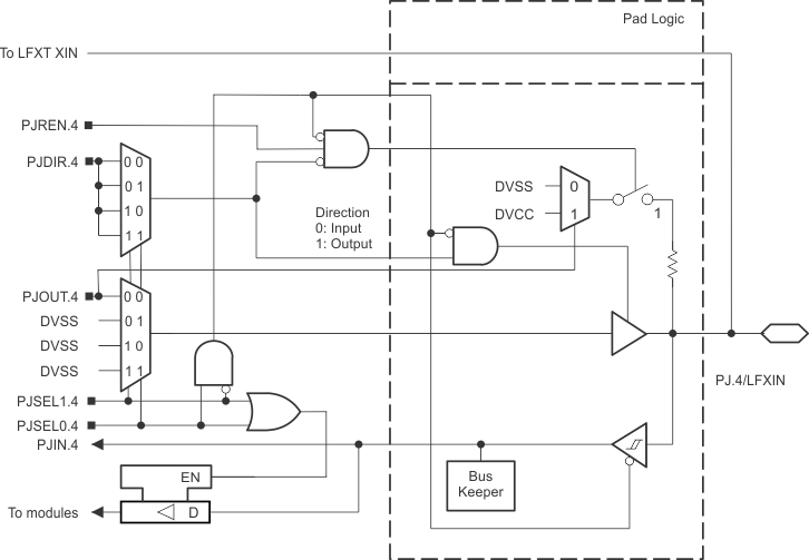
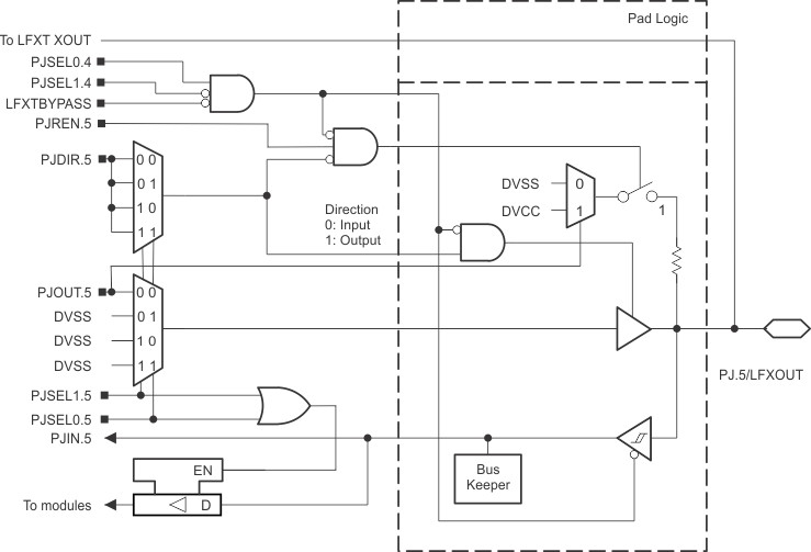
6.14.20 Port PJ (PJ.4 and PJ.5) Input/Output With Schmitt Trigger
Figure 6-21 and Figure 6-22 show the port diagrams. Table 6-43 summarizes the selection of the pin function.

NOTE:
Functional representation only.
NOTE:
Functional representation only.Table 6-43 Port PJ (PJ.4 and PJ.5) Pin Functions
| PIN NAME (PJ.x) | x | FUNCTION | CONTROL BITS AND SIGNALS(1) | |||||
|---|---|---|---|---|---|---|---|---|
| PJDIR.x | PJSEL1.5 | PJSEL0.5 | PJSEL1.4 | PJSEL0.4 | LFXT
BYPASS |
|||
| PJ.4/LFXIN | 4 | PJ.4 (I/O) | I: 0; O: 1 | X | X | 0 | 0 | X |
| N/A | 0 | X | X | 1 | X | X | ||
| Internally tied to DVSS | 1 | |||||||
| LFXIN crystal mode(2) | X | X | X | 0 | 1 | 0 | ||
| LFXIN bypass mode(2) | X | X | X | 0 | 1 | 1 | ||
| PJ.5/LFXOUT | 5 | PJ.5 (I/O) | I: 0; O: 1 | 0 | 0 | 0 | 0 | 0 |
| 1 | X | |||||||
| X | X | 1(3) | ||||||
| N/A | 0 | see(1) | see(1) | 0 | 0 | 0 | ||
| 1 | X | |||||||
| X | X | 1(3) | ||||||
| Internally tied to DVSS | 1 | see(1) | see(1) | 0 | 0 | 0 | ||
| 1 | X | |||||||
| X | X | 1(3) | ||||||
| LFXOUT crystal mode(2) | X | X | X | 0 | 1 | 0 | ||
(1) If PJSEL0.5 = 1 or PJSEL1.5 = 1, the general-purpose I/O functionality is disabled. No input function is available. Configured as output, the pin is actively pulled to zero.
(2) If PJSEL1.4 = 0 and PJSEL0.4 = 1, the general-purpose I/O is disabled. When LFXTBYPASS = 0, PJ.4 and PJ.5 are configured for crystal operation and PJSEL1.5 and PJSEL0.5 are don't care. When LFXTBYPASS = 1, PJ.4 is configured for bypass operation and PJ.5 is configured as general-purpose I/O.
(3) When PJ.4 is configured in bypass mode, PJ.5 is configured as general-purpose I/O.