ZHCSI49C September 2014 – March 2021
PRODUCTION DATA
- 1 特性
- 2 应用
- 3 说明
- 4 Functional Block Diagram
- 5 Revision History
- 6 Device Comparison
- 7 Terminal Configuration and Functions
-
8 Specifications
- 8.1 Absolute Maximum Ratings
- 8.2 ESD Ratings
- 8.3 Recommended Operating Conditions
- 8.4 Active Mode Supply Current (Into VCC) Excluding External Current
- 8.5 Low-Power Mode Supply Currents (Into VCC) Excluding External Current
- 8.6 Thermal Resistance Characteristics
- 8.7
Timing and Switching Characteristics
- 8.7.1 Reset Timing
- 8.7.2 Clock Specifications
- 8.7.3 Wake-up Characteristics
- 8.7.4 I/O Ports
- 8.7.5 Power Management Module
- 8.7.6 Reference Module
- 8.7.7
SD24
- 8.7.7.1 SD24 Power Supply and Recommended Operating Conditions
- 8.7.7.2 SD24 Internal Voltage Reference
- 8.7.7.3 SD24 External Voltage Reference
- 8.7.7.4 SD24 Input Range
- 8.7.7.5 SD24 Performance, Internal Reference (SD24REFS = 1, SD24OSRx = 256)
- 8.7.7.6 SD24 Performance, External Reference (SD24REFS = 0, SD24OSRx = 256)
- 8.7.7.7 Typical Characteristics
- 8.7.8 eUSCI
- 8.7.9 Timer_A
- 8.7.10 Flash
- 8.7.11 Emulation and Debug
- 9 Detailed Description
- 10Applications, Implementation, and Layout
- 11Device and Documentation Support
- 12Mechanical, Packaging, and Orderable Information
封装选项
机械数据 (封装 | 引脚)
散热焊盘机械数据 (封装 | 引脚)
- RHB|32
订购信息
9.11.4 Port P2, P2.3, Input/Output With Schmitt Trigger
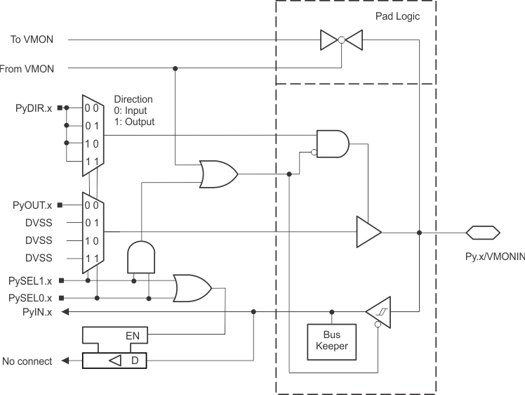
Figure 9-11 shows the pin diagram. Table 9-14 summarizes the selection of the pin function.

Functional representation only.
Figure 9-11 Py.x/VMONIN Pin SchematicTable 9-14 Port P2 (P2.3) Pin Functions
| PIN NAME (P2.x) | x | FUNCTION | CONTROL BITS OR SIGNALS(1) | ||
|---|---|---|---|---|---|
| P2DIR.x | P2SEL1.x | P2SEL0.x | |||
| P2.3/VMONIN | 3 | P2.3 (I/O) | I: 0; O: 1 | 0 | 0 |
| N/A | 0 | 0 | 1 | ||
| DVSS | 1 | ||||
| N/A | 0 | 1 | 0 | ||
| DVSS | 1 | ||||
| VMONIN(2) | X | 1 | 1 | ||
(1) X = Don't care
(2) Setting P2SEL1.3 and P2SEL0.3 disables the output driver and the input Schmitt trigger to prevent parasitic cross currents when applying voltage at VMONIN pin. To enable the VMONIN function, VMONLVLx bits must be set to 3'b111 in the VMONCTL register.