ZHCSI49C September 2014 – March 2021
PRODUCTION DATA
- 1 特性
- 2 应用
- 3 说明
- 4 Functional Block Diagram
- 5 Revision History
- 6 Device Comparison
- 7 Terminal Configuration and Functions
-
8 Specifications
- 8.1 Absolute Maximum Ratings
- 8.2 ESD Ratings
- 8.3 Recommended Operating Conditions
- 8.4 Active Mode Supply Current (Into VCC) Excluding External Current
- 8.5 Low-Power Mode Supply Currents (Into VCC) Excluding External Current
- 8.6 Thermal Resistance Characteristics
- 8.7
Timing and Switching Characteristics
- 8.7.1 Reset Timing
- 8.7.2 Clock Specifications
- 8.7.3 Wake-up Characteristics
- 8.7.4 I/O Ports
- 8.7.5 Power Management Module
- 8.7.6 Reference Module
- 8.7.7
SD24
- 8.7.7.1 SD24 Power Supply and Recommended Operating Conditions
- 8.7.7.2 SD24 Internal Voltage Reference
- 8.7.7.3 SD24 External Voltage Reference
- 8.7.7.4 SD24 Input Range
- 8.7.7.5 SD24 Performance, Internal Reference (SD24REFS = 1, SD24OSRx = 256)
- 8.7.7.6 SD24 Performance, External Reference (SD24REFS = 0, SD24OSRx = 256)
- 8.7.7.7 Typical Characteristics
- 8.7.8 eUSCI
- 8.7.9 Timer_A
- 8.7.10 Flash
- 8.7.11 Emulation and Debug
- 9 Detailed Description
- 10Applications, Implementation, and Layout
- 11Device and Documentation Support
- 12Mechanical, Packaging, and Orderable Information
封装选项
机械数据 (封装 | 引脚)
散热焊盘机械数据 (封装 | 引脚)
- RHB|32
订购信息
9.11.1 Port P1, P1.0 to P1.3, Input/Output With Schmitt Trigger
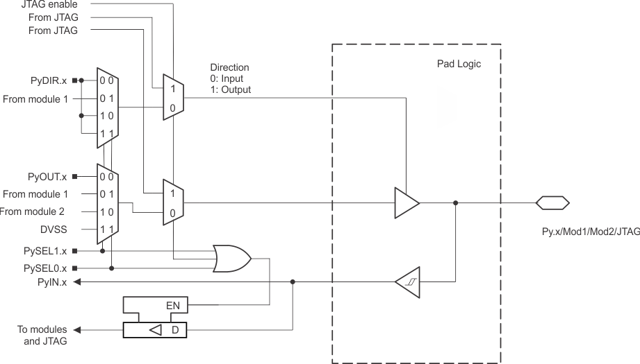
Figure 9-8 shows the pin diagram. Table 9-11 summarizes the selection of the pin function.

Functional representation only.
Figure 9-8 Py.x/Mod1/Mod2/JTAG Pin DiagramTable 9-11 Port P1 (P1.0 to P1.3) Pin Functions
| PIN NAME (P1.x) | x | FUNCTION | CONTROL BITS OR SIGNALS(1) | |||
|---|---|---|---|---|---|---|
| P1DIR.x | P1SEL1.x | P1SEL0.x | JTAG Enable | |||
| P1.0/UCA0STE/MCLK/TCK | 0 | P1.0 (I/O)(2) | I: 0; O: 1 | 0 | 0 | 0 |
| UCA0STE | X(3) | 0 | 1 | 0 | ||
| N/A | 0 | 1 | 0 | 0 | ||
| MCLK | 1 | |||||
| N/A | 0 | 1 | 1 | 0 | ||
| DVSS | 1 | |||||
| TCK(4) | X | X | X | 1 | ||
| P1.1/UCA0CLK/SMCLK/TMS | 1 | P1.1 (I/O)(2) | I: 0; O: 1 | 0 | 0 | 0 |
| UCA0CLK | X(3) | 0 | 1 | 0 | ||
| N/A | 0 | 1 | 0 | 0 | ||
| SMCLK | 1 | |||||
| N/A | 0 | 1 | 1 | 0 | ||
| DVSS | 1 | |||||
| TMS(4) | X | X | X | 1 | ||
| P1.2/UCA0RXD/UCA0SOMI/ ACLK/TDI/TCLK | 2 | P1.2 (I/O)(2) | I: 0; O: 1 | 0 | 0 | 0 |
| UCA0RXD/UCA0SOMI | X(3) | 0 | 1 | 0 | ||
| N/A | 0 | 1 | 0 | 0 | ||
| ACLK | 1 | |||||
| N/A | 0 | 1 | 1 | 0 | ||
| DVSS | 1 | |||||
| TDI/TCLK(4) | X | X | X | 1 | ||
| P1.3/UCA0TXD/UCA0SIMO/ TA0CLK/TDO/TDI | 3 | P1.3 (I/O)(2) | I: 0; O: 1 | 0 | 0 | 0 |
| UCA0TXD/UCA0SIMO | X(3) | 0 | 1 | 0 | ||
| TA0CLK | 0 | 1 | 0 | 0 | ||
| DVSS | 1 | |||||
| N/A | 0 | 1 | 1 | 0 | ||
| DVSS | 1 | |||||
| TDO/TDI(4) | X | X | X | 1 | ||
(1) X = Don't care
(2) Default condition
(3) Direction is controlled by eUSCI_A0 module.
(4) The pin direction is controlled by the JTAG module. The JTAG mode selection is made through the Spy-Bi-Wire 4-wire entry sequence. Neither P1SEL0.x and P1SEL1.x nor P1DIR.x have an effect in these cases.