ZHCSH08 October 2017 MSP432E411Y
PRODUCTION DATA.
- 1器件概述
- 2Revision History
- 3Device Characteristics
- 4Terminal Configuration and Functions
-
5Specifications
- 5.1 Absolute Maximum Ratings
- 5.2 ESD Ratings
- 5.3 Recommended Operating Conditions
- 5.4 Recommended DC Operating Conditions
- 5.5 Recommended GPIO Operating Characteristics
- 5.6 Recommended Fast GPIO Pad Operating Conditions
- 5.7 Recommended Slow GPIO Pad Operating Conditions
- 5.8 GPIO Current Restrictions
- 5.9 I/O Reliability
- 5.10 Current Consumption
- 5.11 Peripheral Current Consumption
- 5.12 LDO Regulator Characteristics
- 5.13 Power Dissipation
- 5.14 Thermal Resistance Characteristics, 212-Pin ZAD (NFBGA) Package
- 5.15
Timing and Switching Characteristics
- 5.15.1 Load Conditions
- 5.15.2 Power Supply Sequencing
- 5.15.3 Reset Timing
- 5.15.4
Clock Specifications
- 5.15.4.1 PLL Specifications
- 5.15.4.2 PIOSC Specifications
- 5.15.4.3 Low-Frequency Oscillator Specifications
- 5.15.4.4 Hibernation Low-Frequency Oscillator Specifications
- 5.15.4.5 Main Oscillator Specifications
- 5.15.4.6 Main Oscillator Specification WIth ADC
- 5.15.4.7 System Clock Characteristics With USB Operation
- 5.15.5 Sleep Modes
- 5.15.6 Hibernation Module
- 5.15.7 Flash Memory
- 5.15.8 EEPROM
- 5.15.9 Input/Output Pin Characteristics
- 5.15.10 External Peripheral Interface (EPI)
- 5.15.11 Analog-to-Digital Converter (ADC)
- 5.15.12 Synchronous Serial Interface (SSI)
- 5.15.13 Inter-Integrated Circuit (I2C) Interface
- 5.15.14
Ethernet Controller
- 5.15.14.1 DC Characteristics
- 5.15.14.2 Clock Characteristics for Ethernet
- 5.15.14.3
AC Characteristics
- Table 5-42 Ethernet Controller Enable and Software Reset Timing
- Table 5-43 MII Serial Management Timing
- Table 5-44 100-Mbps MII Transmit Timing
- Table 5-45 100-Mbps MII Receive Timing
- Table 5-46 100Base-TX Transmit Timing
- Table 5-47 10-Mbps MII Transmit Timing
- Table 5-48 10-Mbps MII Receive Timing
- Table 5-49 10Base-T Normal Link Pulse Timing
- Table 5-50 Auto-Negotiation Fast Link Pulse (FLP) Timing
- Table 5-51 100Base-TX Signal Detect Timing
- Table 5-52 RMII Transmit Timing
- Table 5-53 RMII Receive Timing
- 5.15.15 Universal Serial Bus (USB) Controller
- 5.15.16 LCD Controller
- 5.15.17 Analog Comparator
- 5.15.18 Pulse-Width Modulator (PWM)
- 5.15.19 Emulation and Debug
-
6Detailed Description
- 6.1 Overview
- 6.2 Functional Block Diagram
- 6.3 Arm Cortex-M4F Processor Core
- 6.4 On-Chip Memory
- 6.5
Peripherals
- 6.5.1 External Peripheral Interface (EPI)
- 6.5.2 Cyclical Redundancy Check (CRC)
- 6.5.3 Advanced Encryption Standard (AES) Accelerator
- 6.5.4 Data Encryption Standard (DES) Accelerator
- 6.5.5 Secure Hash Algorithm/Message Digest Algorithm (SHA/MD5) Accelerator
- 6.5.6 Serial Communications Peripherals
- 6.5.7 System Integration
- 6.5.8 LCD Controller
- 6.5.9 Advanced Motion Control
- 6.5.10 Analog
- 6.5.11 JTAG and Arm Serial Wire Debug
- 6.5.12 Peripheral Memory Map
- 6.6 Identification
- 6.7 Boot Modes
- 7Applications, Implementation, and Layout
- 8器件和文档支持
- 9机械、封装和可订购信息
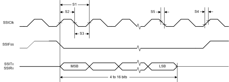
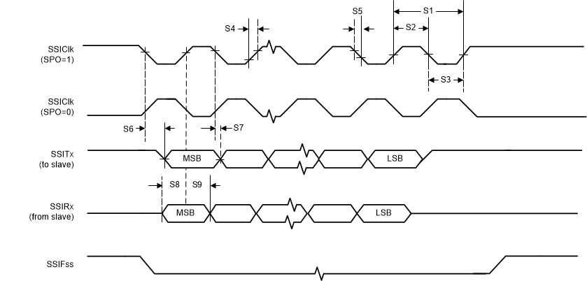
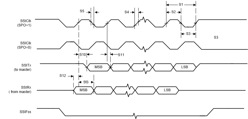
Table 5-35 SSI Characteristics
over operating free-air temperature (unless otherwise noted) (see Figure 5-28, Figure 5-29, and Figure 5-30)| NO. | PARAMETER | MIN | TYP | MAX | UNIT | ||
|---|---|---|---|---|---|---|---|
| S1 | tCLK_PER | SSIClk cycle time | As master(1) | 16.67 | ns | ||
| As slave(2) | 100 | ||||||
| S2 | tCLK_HIGH | SSIClk high time | As master | 8.33 | ns | ||
| As slave | 50 | ||||||
| S3 | tCLK_LOW | SSIClk low time | As master | 8.33 | ns | ||
| As slave | 50 | ||||||
| S4 | tCLKR | SSIClk rise time(3) | 1.25 | ns | |||
| S5 | tCLKF | SSIClk fall time (3) | 1.25 | ns | |||
| S6 | tTXDMOV | Master mode: master Tx data output (to slave) valid time from edge of SSIClk | 4.00 | ns | |||
| S7 | tTXDMOH | Master mode: master Tx data output (to slave) hold time after next SSIClk | 0.60 | ns | |||
| S8 | tRXDMS | Master mode: master Rx data In (from slave) setup time | 7.89 | ns | |||
| S9 | tRXDMH | Master mode: master Rx data In (from slave) hold time | 0 | ns | |||
| S10 | tTXDSOV | Slave mode: master Tx data output (to master) valid time from edge of SSIClk | 47.60(4) | ns | |||
| S11 | tTXDSOH | Slave mode: slave Tx data output (to master) hold time from next SSIClk | 37.4(5) | ns | |||
| S13 | tRXDSSU | Slave mode: Rx data in (from master) setup time | 0 | ns | |||
| S14 | tRXDSH | Slave mode: Rx data in (from master) hold time | 37.03(6) | ns | |||
(1) In master mode, the system clock must be at least twice as fast as the SSIClk.
(2) In slave mode, the system clock must be at least 12 times faster than the SSIClk.
(3) The delays shown are using 12-mA drive strength.
(4) This MAX value is for the minimum slave mode tSYSCLK period (8.33 ns). To find the MAX tTXDSOV value for a larger tSYSCLK, use the equation: 4 × tSYSCLK + 14.25.
(5) This MIN value is for the minimum slave mode tSYSCLK (8.33 ns). To find the MIN tTXDSOH value for a larger tSYSCLK, use the equation: 4 × tSYSCLK + 4.08.
(6) This MIN value is for the minimum slave mode tSYSCLK (8.33 ns). To find the MIN tTXDSH value for a larger tSYSCLK, use the equation: 4 × tSYSCLK + 3.70.
 Figure 5-28 SSI Timing for TI Frame Format (FRF = 01), Single Transfer Timing Measurement
 Figure 5-29 Master Mode SSI Timing for SPI Frame Format (FRF = 00), With SPH = 1
 Figure 5-30 Slave Mode SSI Timing for SPI Frame Format (FRF = 00), With SPH = 1
Table 5-36 lists the characteristics for Bi-SSI and Quad-SSI.