ZHCSFV0C November 2016 – October 2019 MUX36D08 , MUX36S16
PRODUCTION DATA.
- 1 特性
- 2 应用
- 3 说明
- 4 修订历史记录
- 5 Pin Configuration and Functions
- 6 Specifications
- 7 Parameter Measurement Information
- 8 Detailed Description
- 9 Application and Implementation
- 10Power Supply Recommendations
- 11Layout
- 12器件和文档支持
- 13机械、封装和可订购信息
封装选项
机械数据 (封装 | 引脚)
散热焊盘机械数据 (封装 | 引脚)
订购信息
8.3.2 Ultralow Charge Injection
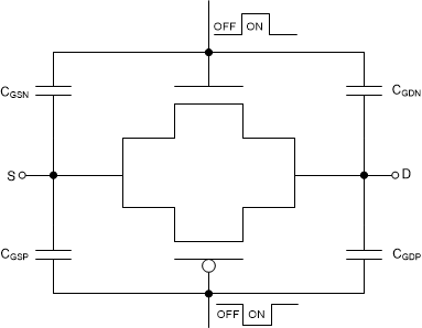
The MUX36xxx have a simple transmission gate topology, as shown in Figure 39. Any mismatch in the stray capacitance associated with the NMOS and PMOS causes an output level change whenever the switch is opened or closed.
 Figure 39. Transmission Gate Topology
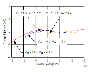
 The MUX36xxx have special charge-injection cancellation circuitry that reduces the source-to-drain charge injection to as low as 0.31 pC at VS = 0 V, and ±0.9 pC in the full signal range, as shown in Figure 40.
 Figure 40. Source-to-Drain Charge Injection
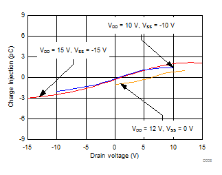
 The drain-to-source charge injection becomes important when the device is used as a demultiplexer (demux), where D becomes the input and Sx becomes the output. Figure 41 shows the drain-to-source charge injection across the full signal range.
 Figure 41. Drain-to-Source Charge Injection