ZHCSDW5A June 2015 – July 2015 ONET1130EC
PRODUCTION DATA.
- 1 特性
- 2 应用
- 3 说明
- 4 修订历史记录
- 5 说明(续)
- 6 Pin Configuration and Function
- 7 Specifications
-
8 Detailed Description
- 8.1 Overview
- 8.2 Functional Block Diagram
- 8.3
Feature Description
- 8.3.1
Transmitter
- 8.3.1.1 Equalizer
- 8.3.1.2 CDR
- 8.3.1.3 Modulator Driver
- 8.3.1.4 Modulation Current Generator
- 8.3.1.5 DC Offset Cancellation and Cross Point Control
- 8.3.1.6 Transmitter Loopback (Electrical Loopback)
- 8.3.1.7 Bias Current Generation and APC Loop
- 8.3.1.8 Laser Safety Features and Fault Recovery Procedure
- 8.3.2 Receiver
- 8.3.3 Analog Block
- 8.3.4 Acknowledge
- 8.3.1
Transmitter
- 8.4 Device Functional Modes
- 8.5 Programming
- 8.6
Register Mapping
- 8.6.1 R/W Control Registers
- 8.6.2
RX Registers
- 8.6.2.1 RX Register 4 (offset = 0000 0000) [reset = 0h]
- 8.6.2.2 RX Register 5 (offset = 0000 0000) [reset = 0h]
- 8.6.2.3 RX Register 6 (offset = 0000 0000) [reset = 0h]
- 8.6.2.4 RX Register 7 (offset = 0000 0000) [reset = 0h]
- 8.6.2.5 RX Register 8 (offset = 0000 0000) [reset = 0h]
- 8.6.2.6 RX Register 9 (offset = 0000 0000) [reset = 0h]
- 8.6.3
TX Registers
- 8.6.3.1 TX Register 10 (offset = 0000 0000) [reset = 0h]
- 8.6.3.2 TX Register 11 (offset = 0000 0000) [reset = 0h]
- 8.6.3.3 TX Register 12 (offset = 0000 0000) [reset = 0h]
- 8.6.3.4 TX Register 13 (offset = 0h) [reset = 0]
- 8.6.3.5 TX Register 14 (offset = 0000 0000) [reset = 0h]
- 8.6.3.6 TX Register 15 (offset = 0000 0000) [reset = 0h]
- 8.6.3.7 TX Register 16 (offset = 0000 0000) [reset = 0h]
- 8.6.3.8 TX Register 17 (offset = 0000 0000) [reset = 0h]
- 8.6.3.9 TX Register 18 (offset = 0000 0000) [reset = 0h]
- 8.6.3.10 TX Register 19 (offset = 0000 0000) [reset = 0h]
- 8.6.4 Reserved Registers
- 8.6.5 Read Only Registers
- 8.6.6 Adjustment Registers
- 9 Application Information and Implementations
- 10Power Supply Recommendations
- 11Layout
- 12器件和文档支持
- 13机械、封装和可订购信息
9 Application Information and Implementations
NOTE
Information in the following applications sections is not part of the TI component specification, and TI does not warrant its accuracy or completeness. TI’s customers are responsible for determining suitability of components for their purposes. Customers should validate and test their design implementation to confirm system functionality.
9.1 Application Information
The ONET1130EC is designed to be used in conjunction with a Transmitter Optical Sub-Assembly (TOSA) and a Receiver Optical Sub-Assembly (ROSA). The ONET1130EC, TOSA, ROSA, microcontroller and power management circuitry will typically be used in an XFP or SFP+ 10 Gbps optical transceiver. Figure 68 shows the ONET1130EC in differential mode of operation modulating a differentially driven Mach Zehnder (MZ) modulator TOSA and Figure 70 and Figure 71 show the device in single-ended output mode with an Electroabsorptive Modulated Laser (EML) TOSA. Figure 70 has the photodiode cathode available and Figure 71 has the photodiode anode available.
9.2 Typical Application, Transmitter Differential Mode
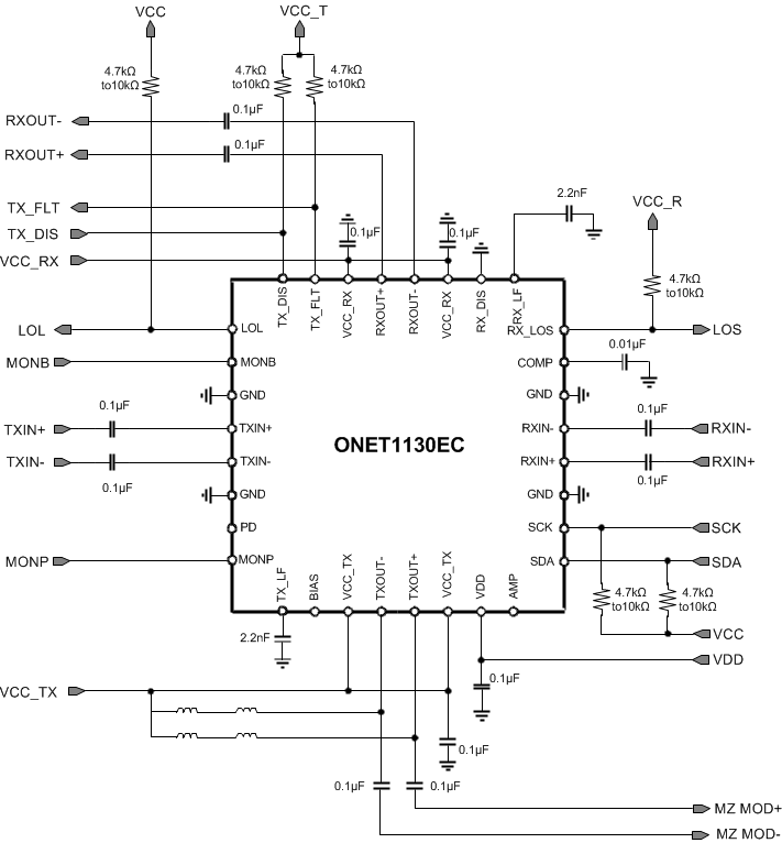 Figure 68. Typical Application Circuit in Differential Mode
9.2.1 Design Requirements
Table 30. Design Parameters
| PARAMETER | VALUE |
|---|---|
| Supply voltage | 2.5 V |
| Transmitter input voltage | 100 mVpp to 1000 mVpp differential |
| Transmitter output voltage | 1 Vpp to 3.6 Vpp differential |
| Receiver input voltage | 6 mVpp to 800 mVpp differential |
| Receiver output voltage | 300 mVpp to 900 mVpp differential |
9.2.2 Detailed Design Procedure
In the transmitter differential mode of operation, the output driver is intended to be used with a differentially driven Mach Zehnder (MZ) modulator TOSA. On the input side, the TXIN+ and TXIN- pins are required to be AC coupled to the signal from the host system and the input voltage should be between 100 mVpp and 1000 mVpp differential. On the output side, the TXOUT+ pin is AC coupled to the modulator positive input and the TXOUT– pin is AC coupled to the modulator negative input. A bias-T from VCC to both the TXOUT+ and TXOUT– pins is required to supply sufficient headroom voltage for the output driver transistors. It is recommended that the inductance in the bias-T have low DC resistance to limit the DC voltage drop and maximize the voltage supplied to the TXOUT+ and TXOUT– pins. If the voltage on these pins drops below approximately 2.1V then the output rise and fall times can be adversely affected.
The receiver inputs, RXIN+ and RXIN–, are AC coupled to the output of ROSA and the input voltage should be between 6 mVpp and 800 mVpp differential. The receiver outputs, RXOUT+ and RXOUT–, are AC coupled to the receiver input of the host system.
9.2.3 Application Curve
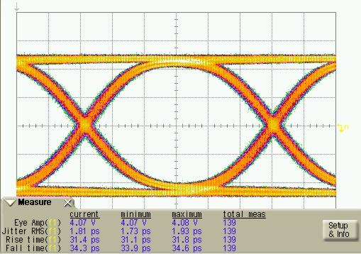 Figure 69. Differential Mode Transmitter Output Eye Diagram
9.2.4 Typical Application, Transmitter Single-Ended Mode
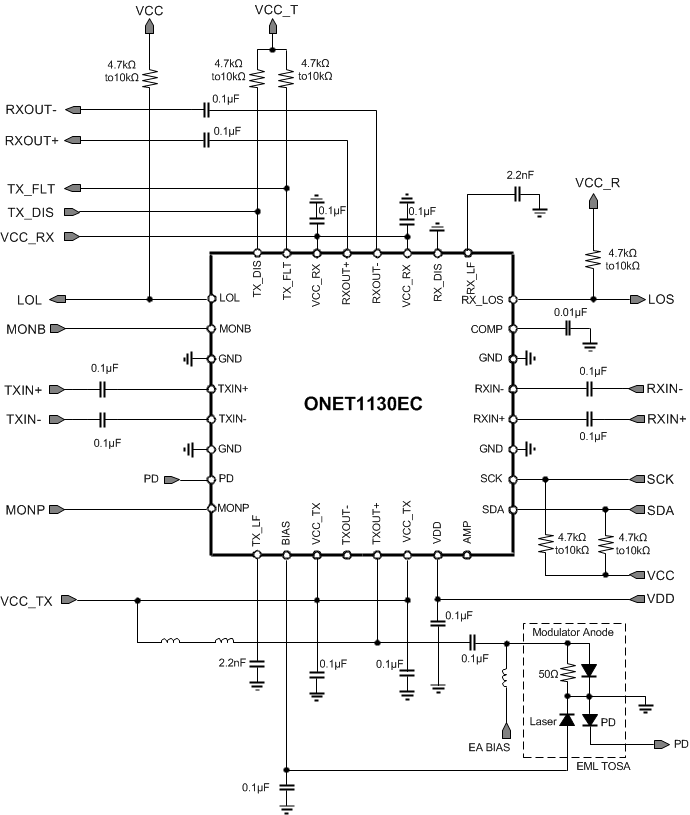 Figure 70. Typical Application Circuit in Single-Ended Mode with an EML and the PD Monitor Cathode Available
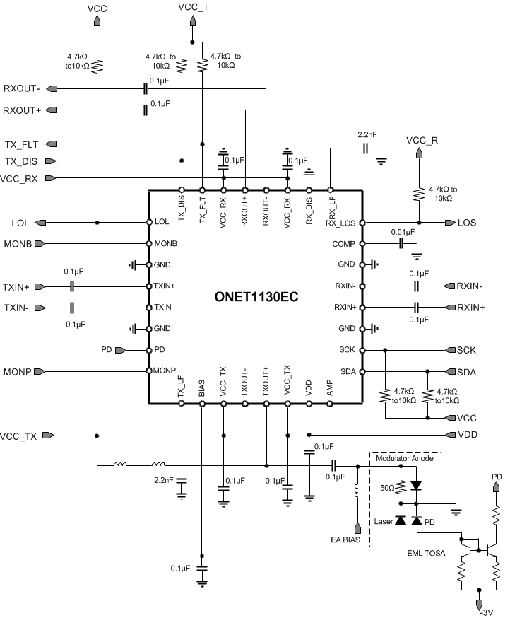 Figure 71. Typical Application Circuit in Single-Ended Mode with an EML and the PD Monitor Anode Available
9.2.4.1 Design Requirements
Table 31. Design Parameters
| PARAMETER | VALUE |
|---|---|
| Supply voltage | 2.5 V |
| Transmitter input voltage | 100 mVpp to 1000 mVpp differential |
| Transmitter output voltage | 0.5 Vpp to 2 Vpp single-ended |
| Receiver input voltage | 6 mVpp to 800 mVpp differential |
| Receiver output voltage | 300 mVpp to 900 mVpp differential |
9.2.4.2 Detailed Design Procedure
In the transmitter single-ended mode of operation, the output driver is intended to be used with a single-ended driven Electroabsorptive Modulated Laser (EML) TOSA. On the input side, the TXIN+ and TXIN– pins are required to be AC coupled to the signal from the host system and the input voltage should be between 100mVpp and 1000mVpp differential. On the output side, it is recommended that the TXOUT+ pin is AC coupled to the modulator input and the TXOUT– pin can be left unterminated or terminated to VCC through a 50Ω resistor. A bias-T from VCC to the TXOUT+ pin is required to supply sufficient headroom voltage for the output driver transistors. It is recommended that the inductance in the bias-T have low DC resistance to limit the DC voltage drop and maximize the voltage supplied to the TXOUT+ pin. If the voltage on this pins drops below approximately 2.1V then the output rise and fall times can be adversely affected.
The receiver inputs, RXIN+ and RXIN–, are AC coupled to the output of ROSA and the input voltage should be between 6mVpp and 800mVpp differential. The receiver outputs, RXOUT+ and RXOUT–, are AC coupled to the receiver input of the host system.
9.2.4.3 Application Curves
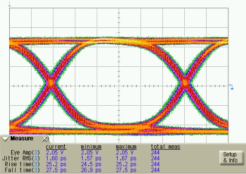 Figure 72. Single-Ended Mode Transmitter Output Eye Diagram