SLLS910A July 2008 – June 2016 ONET8501PB
PRODUCTION DATA.
- 1 Features
- 2 Applications
- 3 Description
- 4 Revision History
- 5 Description (continued)
- 6 Pin Configuration and Functions
- 7 Specifications
-
8 Detailed Description
- 8.1 Overview
- 8.2 Functional Block Diagram
- 8.3 Feature Description
- 8.4 Device Functional Modes
- 8.5 Programming
- 8.6
Register Maps
- 8.6.1 Register 0 (0x00) Mapping - Control Settings
- 8.6.2 Register 1 (0x01) Mapping - Input Threshold Adjust
- 8.6.3 Register 2 (0x02) Mapping - Preemphasis Adjust
- 8.6.4 Register 3 (0x03) Mapping - Output Amplitude Adjust
- 8.6.5 Register 4 (0x04) Mapping - Rate Selection Register A
- 8.6.6 Register 5 (0x05) Mapping - Rate Selection Register B
- 8.6.7 Register 6 (0x06) Mapping - Rate Selection Register C
- 8.6.8 Register 7 (0x07) Mapping - Rate Selection Register D
- 8.6.9 Register 8 (0x08) Mapping - LOS Assert Level Register A
- 8.6.10 Register 9 (0x09) Mapping - LOS Assert Level Register B
- 8.6.11 Register 10 (0x0A) Mapping - LOS Assert Level Register C
- 8.6.12 Register 11 (0x0B) Mapping - LOS Assert Level Register D
- 8.6.13 Register 14 (0x0E) Mapping - Selected Rate Setting (Read Only)
- 8.6.14 Register 15 (0x0F) Mapping - Selected LOS Level (Read Only)
- 9 Application and Implementation
- 10Power Supply Recommendations
- 11Layout
- 12Device and Documentation Support
- 13Mechanical, Packaging, and Orderable Information
9 Application and Implementation
NOTE
Information in the following applications sections is not part of the TI component specification, and TI does not warrant its accuracy or completeness. TI’s customers are responsible for determining suitability of components for their purposes. Customers should validate and test their design implementation to confirm system functionality.
9.1 Application Information
Figure 15 shows a typical application with digital control. In this case DIN+ and DIN– are connected to Transimpedance Amplifier (ROSA) and DOUT+ and DOUT– to SFP connector. SDA and SCK are connected to a microprocessor.
9.2 Typical Application
Figure 15 shows a typical application circuit using the ONET8501PB.
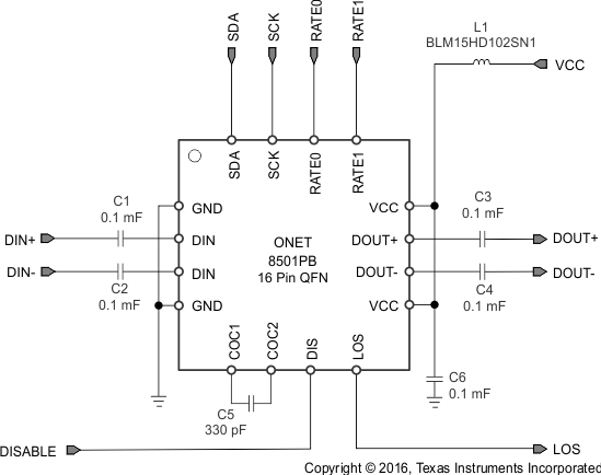 Figure 15. Typical Application Circuit
9.2.1 Design Requirements
For this design example, use the parameters listed in Table 20 as the input parameters.
Table 20. Design Parameters
| PARAMETER | EXAMPLE VALUE |
|---|---|
| Supply voltage | 3.3 V |
| VIN | 20 mVpp to 2000 mVpp |
| Data rate | 8.5 Gbps to 10.3 Gbps |
| AC capacitors | 0.1 µF |
| COC capacitor | 330 pF |
9.2.2 Detailed Design Procedure
The purpose of the series resistors is to improve the signal integrity between the VCSEL driver and the VCSEL. Because the VCSEL impedance varies depending on its type, the series resistor provides a better matching impedance for the modulation current outputs.
The output amplitude adjustments are set as: AMP0 = 1 and AMP1 = 0 (see Register 3). DIN+, DIN–, DOUT+, and DOUT– are AC-coupled with 0.1 µF.
9.2.3 Application Curves
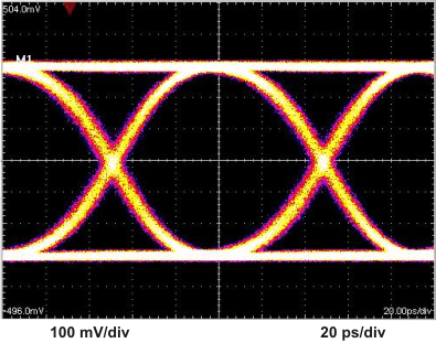 Figure 16. Output Eye-Diagram at 10.3 GBPS vs
and Input Voltage (20 mVpp)
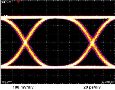 Figure 18. Output Eye-Diagram at 8.5 GBPS
and Input Voltage (20 mVpp)
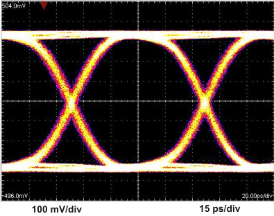 Figure 17. Output Eye-Diagram at 10.3 GBPS vs
and Maximum Input Voltage (2000 mVpp)
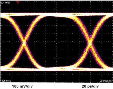 Figure 19. Output Eye-Diagram at 8.5 GBPS
and Maximum Input Voltage (2000 mVpp)