SLLS910A July 2008 – June 2016 ONET8501PB
PRODUCTION DATA.
- 1 Features
- 2 Applications
- 3 Description
- 4 Revision History
- 5 Description (continued)
- 6 Pin Configuration and Functions
- 7 Specifications
-
8 Detailed Description
- 8.1 Overview
- 8.2 Functional Block Diagram
- 8.3 Feature Description
- 8.4 Device Functional Modes
- 8.5 Programming
- 8.6
Register Maps
- 8.6.1 Register 0 (0x00) Mapping - Control Settings
- 8.6.2 Register 1 (0x01) Mapping - Input Threshold Adjust
- 8.6.3 Register 2 (0x02) Mapping - Preemphasis Adjust
- 8.6.4 Register 3 (0x03) Mapping - Output Amplitude Adjust
- 8.6.5 Register 4 (0x04) Mapping - Rate Selection Register A
- 8.6.6 Register 5 (0x05) Mapping - Rate Selection Register B
- 8.6.7 Register 6 (0x06) Mapping - Rate Selection Register C
- 8.6.8 Register 7 (0x07) Mapping - Rate Selection Register D
- 8.6.9 Register 8 (0x08) Mapping - LOS Assert Level Register A
- 8.6.10 Register 9 (0x09) Mapping - LOS Assert Level Register B
- 8.6.11 Register 10 (0x0A) Mapping - LOS Assert Level Register C
- 8.6.12 Register 11 (0x0B) Mapping - LOS Assert Level Register D
- 8.6.13 Register 14 (0x0E) Mapping - Selected Rate Setting (Read Only)
- 8.6.14 Register 15 (0x0F) Mapping - Selected LOS Level (Read Only)
- 9 Application and Implementation
- 10Power Supply Recommendations
- 11Layout
- 12Device and Documentation Support
- 13Mechanical, Packaging, and Orderable Information
11 Layout
11.1 Layout Guidelines
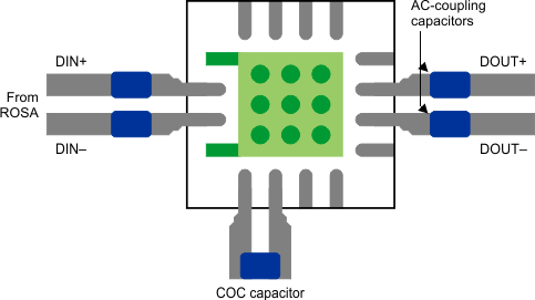
For optimum performance, use 50-Ω transmission lines (100-Ω differential) for connecting the high-speed inputs and outputs. The length of transmission lines must be kept as short as possible to reduce loss and pattern-dependent jitter. TI recommends maximizing the separation of the DOUT+ and DOUT– transmission lines from the DIN+ and DIN– transmission lines to minimize transmitter to receiver crosstalk.
11.2 Layout Example
 Figure 20. ONET8501PB Layout Example