ZHCSRX0H September 1983 – March 2023 OP07 , OP07C , OP07D
PRODUCTION DATA
- 1 特性
- 2 应用
- 3 说明
- 4 Revision History
- 5 Pin Configuration and Functions
- 6 Specifications
- 7 Detailed Description
- 8 Application and Implementation
- 9 Device and Documentation Support
- 10Mechanical, Packaging, and Orderable Information
封装选项
机械数据 (封装 | 引脚)
散热焊盘机械数据 (封装 | 引脚)
订购信息
8.2 Typical Application
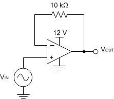
The voltage follower configuration of the operational amplifier is used for applications where a weak signal is used to drive a relatively high current load. This circuit is also called a buffer amplifier or unity gain amplifier. The inputs of an operational amplifier have a very high resistance that puts a negligible current load on the voltage source. The output resistance of the operational amplifier is almost negligible, so the amplifier can provide as much current as necessary to the output load.
 Figure 8-2 Voltage Follower Schematic