ZHCSOD6E December 2003 – August 2023 OPA1632
PRODUCTION DATA
- 1
- 1 特性
- 2 应用
- 3 说明
- 4 Revision History
- 5 Pin Configuration and Functions
- 6 Specifications
- 7 Detailed Description
- 8 Application and Implementation
- 9 Device and Documentation Support
- 10Mechanical, Packaging, and Orderable Information
封装选项
机械数据 (封装 | 引脚)
散热焊盘机械数据 (封装 | 引脚)
- DGN|8
订购信息
8.4.1.1 PowerPAD™ Integrated Circuit Package Design Considerations
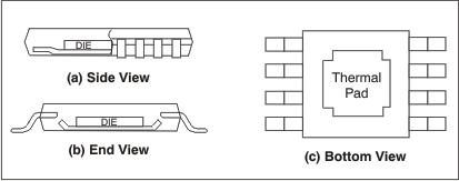
The OPA1632 is available in a thermally-enhanced PowerPAD™ integrated circuit package. This package is constructed using a downset leadframe upon which the die is mounted (see Figure 8-5(a) and Figure 8-5(b)). This arrangement results in the lead frame being exposed as a thermal pad on the underside of the package (see Figure 8-5(c)). Because this thermal pad has direct thermal contact with the die, excellent thermal performance can be achieved by providing a good thermal path away from the thermal pad.
 Figure 8-5 Views of
the Thermally-Enhanced Package
Figure 8-5 Views of
the Thermally-Enhanced PackageThe PowerPAD integrated circuit package allows for both assembly and thermal management in one manufacturing operation. During the surface-mount solder operation (when the leads are being soldered), the thermal pad must be soldered to a copper area underneath the package. Through the use of thermal paths within this copper area, heat can be conducted away from the package into either a ground plane or other heat-dissipating device. Soldering the thermal pad to the printed circuit board (PCB) is always required, even with applications that have low power dissipation. The thermal pad provides the necessary thermal and mechanical connection between the lead frame die pad and the PCB.