ZHCSGB7A June   2017  – November 2017 OPA1641-Q1 , OPA1642-Q1

PRODUCTION DATA.  

  1. 特性
  2. 应用
  3. 说明
    1.     Device Images
      1.      简化内部原理图
      2.      极为稳定的输入电容
  4. 修订历史记录
  5. Pin Configuration and Functions
    1.     Pin Functions: OPA1641-Q1
    2.     Pin Functions: OPA1642-Q1
  6. Specifications
    1. 6.1 Absolute Maximum Ratings
    2. 6.2 ESD Ratings
    3. 6.3 Recommended Operating Conditions
    4. 6.4 Thermal Information
    5. 6.5 Electrical Characteristics
    6. 6.6 Typical Characteristics
  7. Detailed Description
    1. 7.1 Overview
    2. 7.2 Functional Block Diagram
    3. 7.3 Feature Description
      1. 7.3.1 Phase Reversal Protection
      2. 7.3.2 Output Current Limit
      3. 7.3.3 EMI Rejection Ratio (EMIRR)
        1. 7.3.3.1 EMIRR IN+ Test Configuration
    4. 7.4 Device Functional Modes
      1. 7.4.1 Operating Voltage
  8. Application and Implementation
    1. 8.1 Application Information
      1. 8.1.1 Total Harmonic Distortion Measurements
      2. 8.1.2 Source Impedance and Distortion
      3. 8.1.3 Capacitive Load and Stability
      4. 8.1.4 Power Dissipation and Thermal Protection
      5. 8.1.5 Electrical Overstress
    2. 8.2 Typical Application
      1. 8.2.1 Single-Supply Electret Microphone Preamplifier for Speech
        1. 8.2.1.1 Design Requirements
        2. 8.2.1.2 Detailed Design Procedure
        3. 8.2.1.3 Application Curve
  9. Power Supply Recommendations
  10. 10Layout
    1. 10.1 Layout Guidelines
    2. 10.2 Layout Example
  11. 11器件和文档支持
    1. 11.1 器件支持
      1. 11.1.1 开发支持
        1. 11.1.1.1 TINA-TI(免费软件下载)
        2. 11.1.1.2 TI 高精度设计
        3. 11.1.1.3 WEBENCH® 滤波器设计器
    2. 11.2 文档支持
      1. 11.2.1 相关文档
    3. 11.3 相关链接
    4. 11.4 接收文档更新通知
    5. 11.5 社区资源
    6. 11.6 商标
    7. 11.7 静电放电警告
    8. 11.8 Glossary
  12. 12机械、封装和可订购信息

封装选项

机械数据 (封装 | 引脚)
散热焊盘机械数据 (封装 | 引脚)
订购信息

Typical Characteristics

at TA = 25°C, RL = 2 kΩ connected to midsupply, and VCM = VOUT = midsupply (unless otherwise noted)
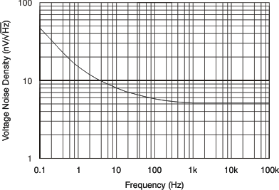
OPA1641-Q1 OPA1642-Q1 tc_v_noise_dens_fqcy_bos484.gif
Figure 1. Input Voltage Noise Density vs Frequency
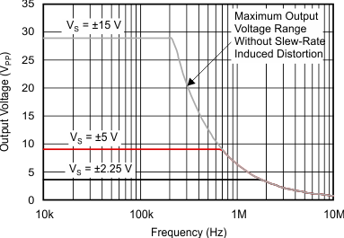
OPA1641-Q1 OPA1642-Q1 tc_vout_max_freq_bos484.gif
Figure 3. Maximum Output Voltage vs Frequency
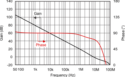
OPA1641-Q1 OPA1642-Q1 tc_gain_phase_fqcy_bos484.gif
Figure 5. Gain and Phase vs Frequency
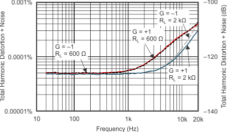
OPA1641-Q1 OPA1642-Q1 tc_thdn_fqcy_01_bos484.gif
VOUT = 3 VRMS BW = 80 kHz
Figure 7. THD+N Ratio vs Frequency
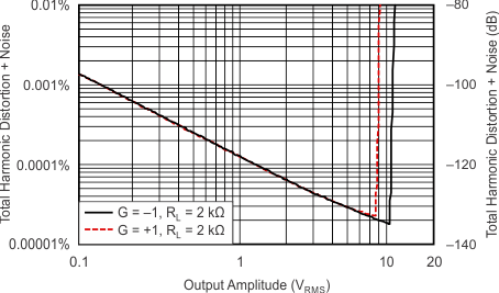
OPA1641-Q1 OPA1642-Q1 tc_thdn_vout_amp_bos484.gif
BW = 80 kHz 1 kHz Signal RSOURCE = 0 Ω
Figure 9. THD+N Ratio vs Output Amplitude
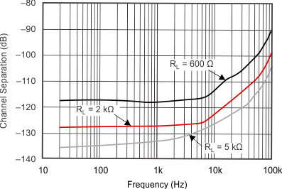
OPA1641-Q1 OPA1642-Q1 tc_chan_sep_fqcy_bos484.gif
VS = ±15 V VOUT = 3 VRMS G = 1
Figure 11. Channel Separation vs Frequency
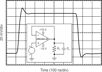
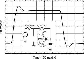
OPA1641-Q1 OPA1642-Q1 tc_sm_signal_step_g1_bos791.gif
G = 1 CL = 100 pF
Figure 13. Small-Signal Step Response (100 mV)
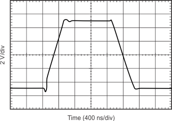
OPA1641-Q1 OPA1642-Q1 tc_lg_signal_step_g1_bos484.gif
G = 1 CL = 100 pF
Figure 15. Large-Signal Step Response
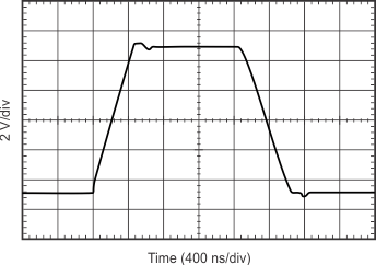
OPA1641-Q1 OPA1642-Q1 tc_pos_overload_recovery_bos791.gif
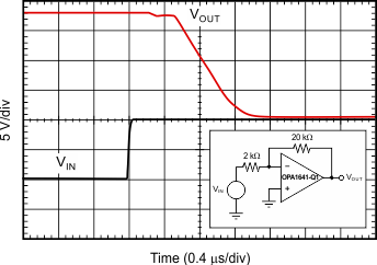
G = –10
Figure 17. Positive Overload Recovery
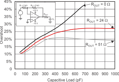
OPA1641-Q1 OPA1642-Q1 tc_sm_sig_ovrsht_cload_01_bos791.gif
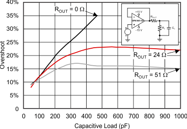
G = 1
Figure 19. Small-Signal Overshoot vs Capacitive Load
(100-mV Output Step)
OPA1641-Q1 OPA1642-Q1 tc_aol_temp_bos484.gif
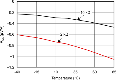
Figure 21. Open-Loop Gain vs Temperature
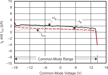
OPA1641-Q1 OPA1642-Q1 tc_ib_ios_cm_v_bos484.gif
VS = ±18 V
Figure 23. IB and IOS vs Common-Mode Voltage
OPA1641-Q1 OPA1642-Q1 tc_iq_vsupply_bos484.gif
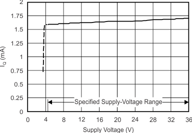
Figure 25. Quiescent Current vs Supply Voltage
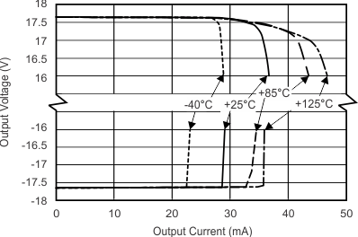
OPA1641-Q1 OPA1642-Q1 tc_vout_iout_bos484.gif
Figure 27. Output Voltage vs Output Current
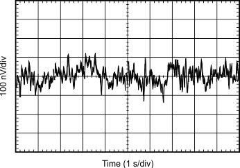
OPA1641-Q1 OPA1642-Q1 tc_noise_bos484.gif
Figure 2. 0.1-Hz to 10-Hz Noise
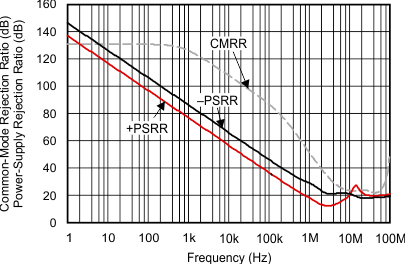
OPA1641-Q1 OPA1642-Q1 tc_cmrr_psrr_fqcy_bos484.gif
Figure 4. CMRR and PSRR vs Frequency
(Referred to Input)
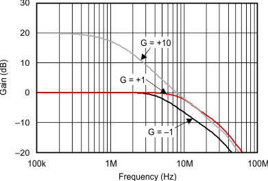
OPA1641-Q1 OPA1642-Q1 tc_closed_lp_gain_fqcy_bos484.gif
Figure 6. Closed-Loop Gain vs Frequency
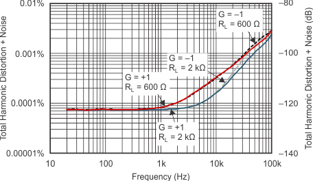
OPA1641-Q1 OPA1642-Q1 tc_thdn_fqcy_03_bos484.gif
VOUT = 3 VRMS BW > 500 kHz
Figure 8. THD+N Ratio vs Frequency
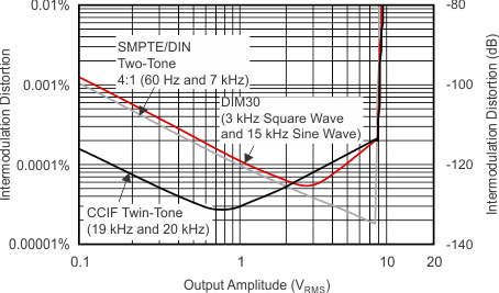
OPA1641-Q1 OPA1642-Q1 tc_imd_out_amp_bos484.gif
G = 1
Figure 10. Intermodulation Distortion
vs Output Amplitude
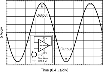
OPA1641-Q1 OPA1642-Q1 tc_phase_reverse_bos791.gif
Figure 12. No Phase Reversal
OPA1641-Q1 OPA1642-Q1 tc_sm_signal_step_g-1_bos791.gif
G = –1 CL = 100 pF
Figure 14. Small-Signal Step Response (100 mV)
OPA1641-Q1 OPA1642-Q1 tc_lg_signal_step_g-1_bos484.gif
G = –1 CL = 100 pF
Figure 16. Large-Signal Step Response
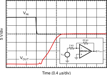
OPA1641-Q1 OPA1642-Q1 tc_neg_overload_recovery_bos791.gif
G = –10
Figure 18. Negative Overload Recovery
OPA1641-Q1 OPA1642-Q1 tc_sm_sig_ovrsht_cload_02_bos791.gif
G = –1
Figure 20. Small-Signal Overshoot vs Capacitive Load
(100-mV Output Step)
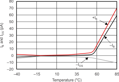
OPA1641-Q1 OPA1642-Q1 tc_ib_ios_temp_bos484.gif
Figure 22. IB and IOS vs Temperature
OPA1641-Q1 OPA1642-Q1 tc_iq_temp_bos484.gif
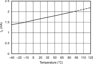
Figure 24. Quiescent Current vs Temperature
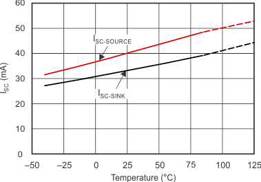
OPA1641-Q1 OPA1642-Q1 tc_isc_temp_bos484.gif
VOUT = Midsupply (includes self-heating)
Figure 26. Short-Circuit Current vs Temperature
OPA1641-Q1 OPA1642-Q1 tc_oloop_freq_bos484.gif
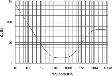
Figure 28. Open-Loop Output Impedance vs Frequency