SBOS484D December 2009 – April 2016 OPA1641 , OPA1642 , OPA1644
PRODUCTION DATA.
- 1 Features
- 2 Applications
- 3 Description
- 4 Revision History
- 5 Pin Configuration and Functions
- 6 Specifications
- 7 Detailed Description
- 8 Application and Implementation
- 9 Power Supply Recommendations
- 10Layout
- 11Device and Documentation Support
- 12Mechanical, Packaging, and Orderable Information
7 Detailed Description
7.1 Overview
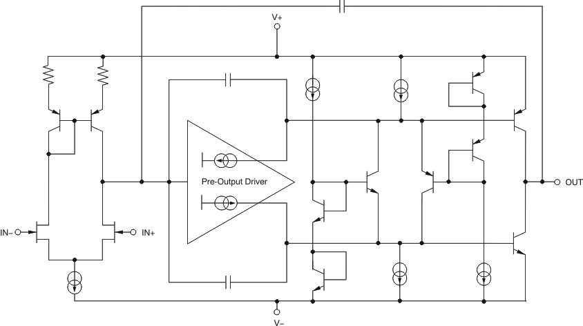
The OPA164x family of operational amplifiers combine an ultra low noise JFET input stage with a rail-to-rail output stage to provide high overall performance in audio applications. The internal topology is selected specifically to deliver extremely low distortion, consume limited power, and accommodate small packages. These amplifiers are well-suited for analog signal processing applications such as active filter circuits, pre-amplifiers, and tone controls. The unique input stage design and semiconductor processes used in this device deliver extremely high performance even in applications with high source impedance and wide common-mode voltage swings.
7.2 Functional Block Diagram

7.3 Feature Description
7.3.1 Phase Reversal Protection
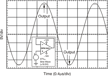
The OPA164x family has internal phase-reversal protection. Many op amps exhibit phase reversal when the input is driven beyond the linear common-mode range. This condition is most often encountered in noninverting circuits when the input is driven beyond the specified common-mode voltage range, causing the output to reverse into the opposite rail. The input of the OPA164x prevents phase reversal with excessive common-mode voltage. Instead, the appropriate rail limits the output voltage. This performance is shown in Figure 29.
 Figure 29. Output Waveform Devoid of Phase Reversal During an Input Overdrive Condition
7.3.2 Output Current Limit
The output current of the OPA164x series is limited by internal circuitry to 36 mA and –30 mA (sourcing and sinking), to protect the device if the output is accidentally shorted. This short-circuit current depends on temperature; see Figure 26.
Although uncommon for most modern audio applications to require 600-Ω load drive capability, many audio operational amplifier applications continue to specify the total harmonic distortion (THD+N) at 600-Ω load for comparative purposes. Figure 7 and Figure 8 provide typical THD+N measurement curves for the OPA164x series, where the output drives a 3-VRMS signal into a 600-Ω load. However, correct device operation cannot be ensured when driving 600-Ω loads at full supply. Depending on supply voltage and temperature, this operating condition can possibly trigger the output current limit circuitry of the device.
7.3.3 EMI Rejection Ratio (EMIRR)
The electromagnetic interference (EMI) rejection ratio, or EMIRR, describes the EMI immunity of operational amplifiers. An adverse effect that is common to many operational amplifiers is a change in the offset voltage as a result of RF signal rectification. An operational amplifier that is more efficient at rejecting this change in offset as a result of EMI has a higher EMIRR and is quantified by a decibel value. Measuring EMIRR can be performed in many ways, but this document provides the EMIRR IN+, which specifically describes the EMIRR performance when the RF signal is applied to the noninverting input pin of the operational amplifier. In general, only the noninverting input is tested for EMIRR for the following three reasons:
- Operational amplifier input pins are known to be the most sensitive to EMI, and typically rectify RF signals better than the supply or output pins.
- The noninverting and inverting operational amplifier inputs have symmetrical physical layouts and exhibit nearly matching EMIRR performance.
- EMIRR is easier to measure on noninverting pins than on other pins because the noninverting input pin can be isolated on a printed-circuit-board (PCB). This isolation allows the RF signal to be applied directly to the noninverting input pin with no complex interactions from other components or connecting PCB traces.
A more formal discussion of the EMIRR IN+ definition and test method is provided in application report EMI Rejection Ratio of Operational Amplifiers (SBOA128), available for download at www.ti.com.
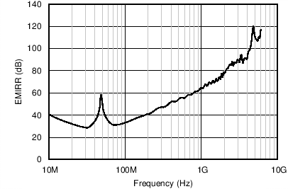
The EMIRR IN+ of the OPA164x is plotted versus frequency in Figure 30. If available, any dual and quad operational amplifier device versions have nearly identical EMIRR IN+ performance. The OPA164x unity-gain bandwidth is 11 MHz. EMIRR performance below this frequency denotes interfering signals that fall within the operational amplifier bandwidth.
 Figure 30. OPA164x EMIRR vs Frequency
Table 1 lists the EMIRR IN+ values for the OPA164x at particular frequencies commonly encountered in real-world applications. Applications listed in Table 1 can be centered on or operated near the particular frequency shown. This information can be of special interest to designers working with these types of applications, or working in other fields likely to encounter RF interference from broad sources, such as the industrial, scientific, and medical (ISM) radio band.
Table 1. OPA164x EMIRR IN+ for Frequencies of Interest
| FREQUENCY | APPLICATION, ALLOCATION | EMIRR IN+ |
|---|---|---|
| 400 MHz | Mobile radio, mobile satellite, space operation, weather, radar, UHF | 53.1 dB |
| 900 MHz | GSM, radio communication and navigation, GPS (to 1.6 GHz), ISM, aeronautical mobile, UHF |
72.2 dB |
| 1.8 GHz | GSM, mobile personal comm. broadband, satellite, L-band | 80.7 dB |
| 2.4 GHz | 802.11b/g/n, Bluetooth™, mobile personal comm., ISM, amateur radio and satellite, S-band | 86.8 dB |
| 3.6 GHz | Radiolocation, aero comm./nav., satellite, mobile, S-band | 91.7 dB |
| 5 GHz | 802.11a/n, aero communication and navigation, mobile communication, space and satellite operation, C-band |
96.6 dB |
7.3.3.1 EMIRR IN+ Test Configuration
Figure 31 shows the circuit configuration for testing the EMIRR IN+. An RF source is connected to the operational amplifier noninverting input pin using a transmission line. The operational amplifier is configured in a unity-gain buffer topology with the output connected to a low-pass filter (LPF) and a digital multimeter (DMM). A large impedance mismatch at the operational amplifier input causes a voltage reflection; however, this effect is characterized and accounted for when determining the EMIRR IN+. The resulting dc offset voltage is sampled and measured by the multimeter. The LPF isolates the multimeter from residual RF signals that can interfere with multimeter accuracy. See EMI Rejection Ratio of Operational Amplifiers (SBOA128) for more details.
 Figure 31. EMIRR IN+ Test Configuration Schematic
7.4 Device Functional Modes
7.4.1 Operating Voltage
The OPA1641, OPA1642, and OPA1644 series of operational amplifiers can be used with single or dual supplies from an operating range of VS = 4.5 V (±2.25 V) and up to VS = 36 V (±18 V). These devices do not require symmetrical supplies; only a minimum supply voltage of 4.5 V (±2.25 V) is required. For VS less than ±3.5 V, the common-mode input range does not include midsupply. Supply voltages higher than 40 V can permanently damage the device; see the Absolute Maximum Ratings table for more information. Key parameters are specified over the operating temperature range, TA = –40°C to +85°C. Key parameters that vary over the supply voltage or temperature range are illustrated in the Typical Characteristics section.