ZHCS618B December 2011 – December 2016 OPA1652 , OPA1654
PRODUCTION DATA.
- 1 特性
- 2 应用
- 3 说明
- 4 修订历史记录
- 5 Pin Configuration and Functions
- 6 Specifications
- 7 Detailed Description
- 8 Application and Implementation
- 9 Power Supply Recommendations
- 10Layout
- 11器件和文档支持
- 12机械、封装和可订购信息
封装选项
机械数据 (封装 | 引脚)
散热焊盘机械数据 (封装 | 引脚)
- DRG|8
订购信息
7 Detailed Description
7.1 Overview
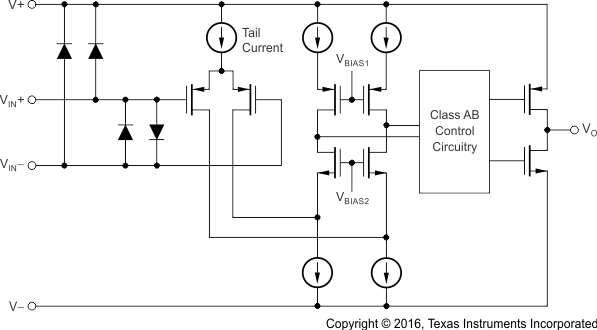
The OPA1652 and OPA1654 are unity-gain stable, precision dual and quad op amps with very low noise. The Functional Block Diagram shows a simplified schematic of the OPA165x (with one channel shown). The device consists of a very low noise input stage with a folded cascode and a rail-to-rail output stage. This topology exhibits superior noise and distortion performance across a wide range of supply voltages not previously delivered by audio operational amplifiers.
7.2 Functional Block Diagram

7.3 Feature Description
7.3.1 Phase Reversal Protection
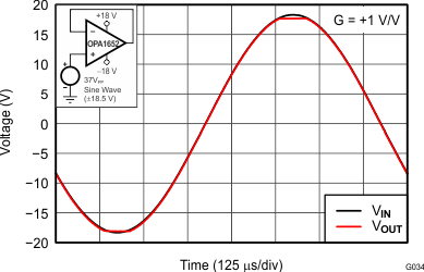
The OPA165x family has internal phase-reversal protection. Many op amps exhibit phase reversal when the input is driven beyond the linear common-mode range. This condition is most often encountered in noninverting circuits when the input is driven beyond the specified common-mode voltage range, causing the output to reverse into the opposite rail. The input of the OPA165x prevents phase reversal with excessive common-mode voltage. Instead, the appropriate rail limits the output voltage. This performance is shown in Figure 35.
 Figure 35. Output Waveform Devoid of Phase Reversal During an Input Overdrive Condition
7.3.2 Input Protection
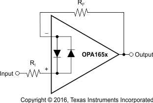
The input terminals of the OPA1652 and OPA1654 are protected from excessive differential voltage with back-to-back diodes, as Figure 36 illustrates. In most circuit applications, the input protection circuitry has no consequence. However, in low-gain or G = 1 circuits, fast ramping input signals can forward bias these diodes because the output of the amplifier cannot respond rapidly enough to the input ramp. If the input signal is fast enough to create this forward bias condition, the input signal current must be limited to 10 mA or less. If the input signal current is not inherently limited, an input series resistor (RI) or a feedback resistor (RF) can limit the signal input current. This resistor degrades the low-noise performance of the OPA165x, and is examined in the Noise Performance section. Figure 36 shows an example configuration when both current-limiting input and feedback resistors are used.
 Figure 36. Pulsed Operation
7.3.3 Electrical Overstress
Designers typically ask questions about the capability of an operational amplifier to withstand electrical overstress. These questions tend to focus on the device inputs, but can involve the supply voltage pins or the output pin. Each of these different pin functions have electrical stress limits determined by the voltage breakdown characteristics of the particular semiconductor fabrication process and specific circuits connected to the pin. Additionally, internal electrostatic discharge (ESD) protection is built into these circuits to protect them from accidental ESD events both before and during product assembly.
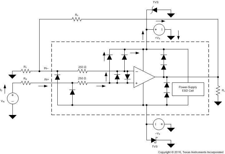
A good understanding of this basic ESD circuitry and the relevance to an electrical overstress event is helpful. Figure 37 illustrates the ESD circuits contained in the OPA165x (indicated by the dashed line area). The ESD protection circuitry involves several current-steering diodes connected from the input and output pins and routed back to the internal power-supply lines, where the diodes meet at an absorption device internal to the operational amplifier. This protection circuitry is intended to remain inactive during normal circuit operation.
 Figure 37. Equivalent Internal ESD Circuitry Relative to a Typical Circuit Application
An ESD event produces a short-duration, high-voltage pulse that is transformed into a short-duration, high-current pulse when discharging through a semiconductor device. The ESD protection circuits are designed to provide a current path around the operational amplifier core to prevent damage. The energy absorbed by the protection circuitry is then dissipated as heat.
When an ESD voltage develops across two or more amplifier device pins, current flows through one or more steering diodes. The absorption device activates depending on the path that the current takes. The absorption device has a trigger, or threshold voltage, that is above the normal operating voltage of the OPA165x, but below the device breakdown voltage level. When this threshold is exceeded, the absorption device quickly activates and clamps the voltage across the supply rails to a safe level.
When the operational amplifier connects into a circuit (refer to Figure 37), the ESD protection components are intended to remain inactive and do not become involved in the application circuit operation. However, circumstances may arise where an applied voltage exceeds the operating voltage range of a given pin. If this condition occurs, there is a risk that some internal ESD protection circuits can turn on and conduct current. Any such current flow occurs through steering-diode paths and rarely involves the absorption device.
Figure 37 shows a specific example where the input voltage (VIN) exceeds the positive supply voltage (V+) by 500 mV or more. Much of what happens in the circuit depends on the supply characteristics. If V+ can sink the current, one of the upper input steering diodes conducts and directs current to V+. Excessively high current levels can flow with increasingly higher VIN. As a result, the data sheet specifications recommend that applications limit the input current to 10 mA.
If the supply is not capable of sinking the current, VIN begins sourcing current to the operational amplifier, and then becomes the source of positive supply voltage. The danger in this case is that the voltage can rise to levels that exceed the absolute maximum ratings of the operational amplifier.
Another common question explains what happens to the amplifier if an input signal is applied to the input when the power supplies (V+ or V–) are at 0 V. This depends on the supply characteristic when at 0 V, or at a level below the input signal amplitude. If the supplies appear as high impedance, then the input source supplies the operational amplifier current through the current-steering diodes. This state is not a normal bias condition; most likely, the amplifier does not operate normally. If the supplies are at low impedance, then the current through the steering diodes can become quite high. The current level depends on the ability of the input source to deliver current, and any resistance in the input path.
If there is any uncertainty about the ability of the supply to absorb this current, add external Zener diodes to the supply pins; see Figure 37. Select the Zener voltage so the diode does not turn on during normal operation. However, the Zener voltage must be low enough so that the Zener diode conducts if the supply pin rises above the safe-operating, supply-voltage level.
7.4 Device Functional Modes
7.4.1 Operating Voltage
The OPA165x series op amps operate from ±2.25 V to ±18 V supplies while maintaining excellent performance. The OPA165x series can operate with as little as 4.5 V between the supplies and with up to 36 V between the supplies. However, some applications do not require equal positive and negative output voltage swing. With the OPA165x series, power-supply voltages do not need to be equal. For example, the positive supply can be set to 25 V with the negative supply at –5 V.
In all cases, the common-mode voltage must be maintained within the specified range. In addition, key parameters are assured over the specified temperature range of TA = –40°C to +85°C. Parameters that vary significantly with operating voltage or temperature are shown in the Typical Characteristics section.