ZHCSA99C July 2012 – August 2016 OPA1662-Q1
PRODUCTION DATA.
9 Application and Implementation
NOTE
Information in the following applications sections is not part of the TI component specification, and TI does not warrant its accuracy or completeness. TI’s customers are responsible for determining suitability of components for their purposes. Customers should validate and test their design implementation to confirm system functionality.
9.1 Application Information
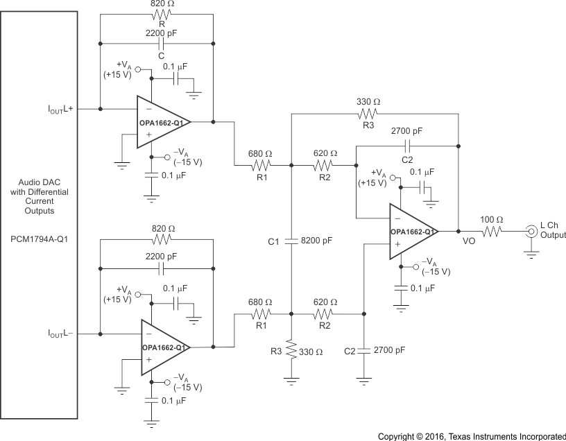
The OPA1662-Q1 is a unity-gain stable, precision dual op amp with very low noise. Applications with noisy or high-impedance power supplies require decoupling capacitors close to the device pins. In most cases, 0.1-µF capacitors are adequate. Figure 43 shows a simplified schematic of the OPA1662-Q1 (one channel shown) while Figure 49 shows an additional application idea.
9.2 Typical Application
 Figure 49. Audio DAC Current to Voltage Converter and Output Filter
9.2.1 Design Requirements
Table 1 lists the design parameters for this example.
Table 1. Design Parameters
| PARAMETER | EXAMPLE VALUE |
|---|---|
| Supply voltage | ±15 V to ±36 V |
| Differential input currents | 0 mA to 30 mA |
| Resistors value tolerance | 1% |
| Ceramic capacitor | XR5 or XR7 50 V |
9.2.2 Detailed Design Procedure
This circuit is designed for converting differential input current into a single ended output voltage. The resistor values are chosen to be relatively low for minimizing the total circuit noise. The filtering capacitors are chosen to maintain adequate bandwidth from 10 Hz to 20 kHz for audio signals.
The first stage converts the audio DAC output current into a voltage with a gain calculated by Equation 1:

where
- R = 820 Ω
- C = 2200 pF
- S is Laplace variable
RC filters the audio DAC output ripple and cutoff frequency =  = 80 KHz
The second differential stage transfer function is calculated by Equation 2:

The denominator of this transfer function  is a quadratic equation and the general form is calculated by Equation 3:

where
- ωo = 2πFo is the resonance frequency
- and Q is the quality factor
The gain peak depends on the quality factor in Equation 4:

The resonance frequency is calculated by Equation 5:

These equations help to maintain adequate bandwidth and keep the differential gain flat so the quality factor is from 0.7 to 1. The resonance frequency must be at least twice the desired bandwidth.
The chosen components give a quality factor of 0.89 and a resonance frequency of 53 KHz.
The overall transfer function is shown in Equation 6:

The  and is 398 mV/mA.
The poles are at 53 KHz and 80 KHz.
9.2.3 Application Curves

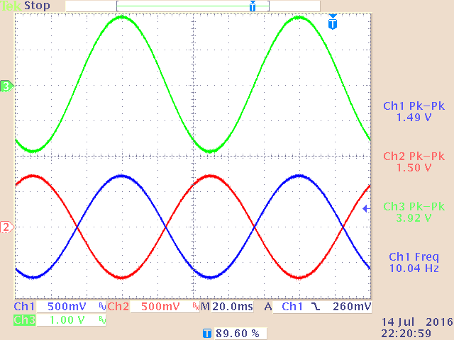
| CH1 = positive input current IOUTL+ = 1.5 V / 150 Ω | ||
| CH2 = negative input current IOUTL– = 1.5 V / 150 Ω | ||
| CH3 = output single-ended voltage |

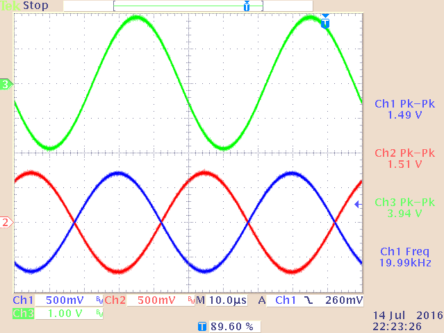
| CH1 = positive input current IOUTL+ = 1.5 V / 150 Ω | ||
| CH2 = negative input current IOUTL– = 1.5 V / 150 Ω | ||
| CH3 = output single-ended voltage |