ZHCSJ01B January   2019  – August 2019 OPA1671

PRODUCTION DATA.  

  1. 特性
  2. 应用
  3. 说明
    1.     Device Images
      1.      驻极体麦克风前置放大器
      2.      OPA1671 电压噪声密度
  4. 修订历史记录
  5. Pin Configuration and Functions
    1.     Pin Functions
  6. Specifications
    1. 6.1 Absolute Maximum Ratings
    2. 6.2 ESD Ratings
    3. 6.3 Recommended Operating Conditions
    4. 6.4 Thermal Information
    5. 6.5 Electrical Characteristics
    6. 6.6 Typical Characteristics
  7. Detailed Description
    1. 7.1 Overview
    2. 7.2 Functional Block Diagram
    3. 7.3 Feature Description
      1. 7.3.1 Operating Voltage
      2. 7.3.2 Input Bias Current
      3. 7.3.3 Common-Mode Voltage Range
      4. 7.3.4 EMI Susceptibility and Input Filtering
    4. 7.4 Device Functional Modes
  8. Application and Implementation
    1. 8.1 Application Information
      1. 8.1.1 Capacitive Loads
      2. 8.1.2 Noise Performance
      3. 8.1.3 Basic Noise Calculations
    2. 8.2 Typical Application
      1. 8.2.1 Design Requirements
      2. 8.2.2 Detailed Design Procedure
      3. 8.2.3 Application Curves
  9. Power Supply Recommendations
  10. 10Layout
    1. 10.1 Layout Guidelines
    2. 10.2 Layout Example
  11. 11器件和文档支持
    1. 11.1 器件支持
      1. 11.1.1 开发支持
        1. 11.1.1.1 TINA-TI(免费软件下载)
    2. 11.2 文档支持
      1. 11.2.1 相关文档
    3. 11.3 接收文档更新通知
    4. 11.4 社区资源
    5. 11.5 商标
    6. 11.6 静电放电警告
    7. 11.7 Glossary
  12. 12机械、封装和可订购信息

封装选项

机械数据 (封装 | 引脚)
散热焊盘机械数据 (封装 | 引脚)
订购信息

Noise Performance

Figure 31 shows the total circuit noise for varying source impedances with the operational amplifier in a unity-gain configuration (with no feedback resistor network and therefore no additional noise contributions). The op amp itself contributes a voltage noise component and a current noise component. The voltage noise is commonly modeled as a time-varying component of the offset voltage. The current noise is modeled as the time-varying component of the input bias current and reacts with the source resistance to create a voltage component of noise. For a CMOS-input device, the noise resulting from the input current is negligible; therefore, the total noise is dominated by the voltage noise of the OPA1671 at low source resistance, and the resistor noise > 1 kΩ.

Figure 31 shows the calculation of the total circuit noise, with these parameters:

  • en = voltage noise
  • RS = source impedance
  • k = Boltzmann's constant = 1.38 × 10⁻²³ J/K
  • T = temperature in kelvins (K)

For more details on calculating noise, see Basic Noise Calculations.
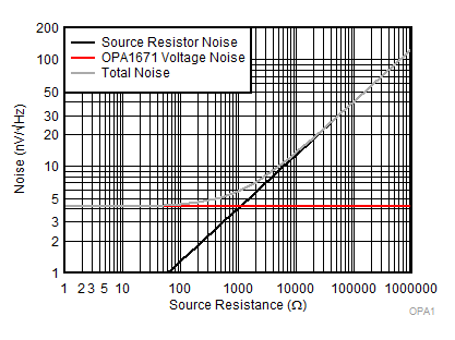
OPA1671 OPA1671_NoiseVoltageContribution2.gifFigure 32. Noise Performance of the OPA1671 in a Unity-Gain Buffer Configuration