ZHCSH60C June   2017  – October 2018 OPA1692

PRODUCTION DATA.  

  1. 特性
  2. 应用
  3. 说明
    1.     Device Images
      1. 3 线制驻极体麦克风的前置放大器
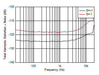
      2.      THD + N 与频率之间的关系(3 VRMS,2kΩ 负载)
  4. 修订历史记录
  5. Pin Configuration and Functions
    1.     Pin Functions: OPA1692
  6. Specifications
    1. 6.1 Absolute Maximum Ratings
    2. 6.2 ESD Ratings
    3. 6.3 Recommended Operating Conditions
    4. 6.4 Thermal Information: OPA1692
    5. 6.5 Electrical Characteristics
    6. 6.6 Typical Characteristics
  7. Detailed Description
    1. 7.1 Overview
    2. 7.2 Functional Block Diagram
    3. 7.3 Feature Description
      1. 7.3.1 Distortion Reduction
      2. 7.3.2 Phase Reversal Protection
      3. 7.3.3 Electrical Overstress
    4. 7.4 Device Functional Modes
      1. 7.4.1 Operating Voltage
  8. Application and Implementation
    1. 8.1 Application Information
      1. 8.1.1 Capacitive Loads
      2. 8.1.2 Noise Performance
      3. 8.1.3 Basic Noise Calculations
      4. 8.1.4 EMI Rejection
      5. 8.1.5 EMIRR +IN Test Configuration
    2. 8.2 Typical Application
      1. 8.2.1 Design Requirements
      2. 8.2.2 Detailed Design Procedure
      3. 8.2.3 Application Curves
    3. 8.3 Other Application Examples
      1. 8.3.1 Two-Wire Electret Microphone Preamplifier
      2. 8.3.2 Battery-Powered Preamplifier for Professional Microphones
  9. Power Supply Recommendations
  10. 10Layout
    1. 10.1 Layout Guidelines
    2. 10.2 Layout Example
    3. 10.3 Power Dissipation
  11. 11器件和文档支持
    1. 11.1 器件支持
      1. 11.1.1 开发支持
        1. 11.1.1.1 TINA-TI™(免费软件下载)
        2. 11.1.1.2 DIP 适配器 EVM
        3. 11.1.1.3 通用运算放大器评估模块 (EVM)
        4. 11.1.1.4 智能放大器扬声器特性鉴定板评估模块
        5. 11.1.1.5 TI 高精度设计
        6. 11.1.1.6 WEBENCH滤波器设计器
    2. 11.2 文档支持
      1. 11.2.1 相关文档
    3. 11.3 相关链接
    4. 11.4 接收文档更新通知
    5. 11.5 社区资源
    6. 11.6 商标
    7. 11.7 静电放电警告
    8. 11.8 术语表
  12. 12机械、封装和可订购信息

封装选项

机械数据 (封装 | 引脚)
散热焊盘机械数据 (封装 | 引脚)
订购信息

Typical Characteristics

at TA = 25°C, VS = ±18 V, and RL = 2 kΩ (unless otherwise noted)
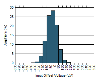
OPA1692 D204_SBOS566.gif
N = 1160 Mean = –139.2 µV Std. Dev. = 105.4 µV
Figure 1. Input Offset Voltage Distribution
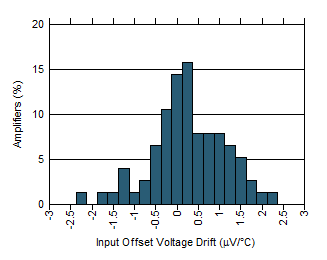
OPA1692 D013_SBOS566.gif
Figure 3. Offset Voltage Drift Distribution
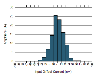
OPA1692 D207_SBOS566.gif
N = 1160 Mean = 0.07 nA Std. Dev. = 1.58 nA
Figure 5. Input Offset Current Distribution
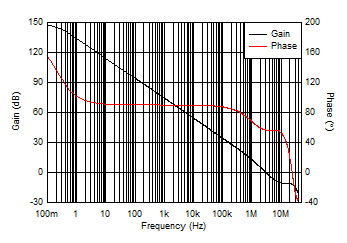
OPA1692 D017_SBOS566.gif
Figure 7. Open-Loop Gain and Phase vs Frequency
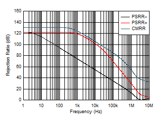
OPA1692 D023_SBOS566.gif
Figure 9. CMRR and PSRR vs Frequency (Referred to Input)
OPA1692 C004_SBOS566.png
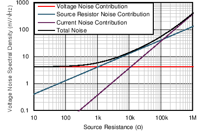
Figure 11. Voltage Noise vs Source Resistance
OPA1692 C007_SBOS566.png
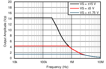
Figure 13. Maximum Output Voltage vs Frequency
OPA1692 D022_SBOS566.gif
G = 1
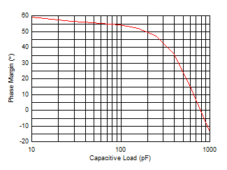
Figure 15. Phase Margin vs Capacitive Load
OPA1692 D039_SBOS566.gif
G = –1 10-mV input step
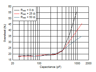
Figure 17. Overshoot vs Capacitive Load
OPA1692 D028_SBOS566.gif
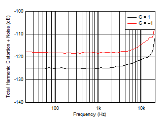
VOUT = 3 VRMS RL = 600 Ω 80-kHz bandwidth
Figure 19. THD + N Ratio vs Frequency
OPA1692 D019_SBOS566.gif
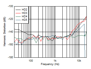
VOUT = 3 VRMS G = 1 80-kHz bandwidth
Figure 21. Distortion Harmonics vs Frequency
OPA1692 D024_SBOS566.gif
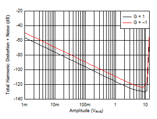
f = 1 kHz 80-kHz bandwidth
Figure 23. THD + N Ratio vs Output Amplitude
OPA1692 D021_SBOS566.gif
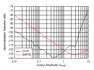
80-kHz bandwidth
Figure 25. Intermodulation Distortion vs Output Amplitude
OPA1692 D202_SBOS901.gif
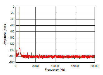
f = 1 kHz VO = 3 VRMS RL = 600 Ω
Figure 27. 1-kHz Output Spectrum
OPA1692 D036_SBOS566.gif
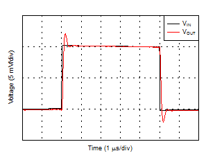
100-pF capacitive load 10-mV input step G = 1
Figure 29. Small-Signal Step Response
OPA1692 D034_SBOS566.gif
100-pF capacitive load 10-V input step G = 1
Figure 31. Large-Signal Step Response
OPA1692 D040_SBOS566.gif
Figure 33. Settling Time
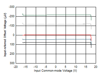
OPA1692 D015_SBOS566.gif
5 typical units
Figure 35. Input Offset Voltage vs Common-Mode Voltage
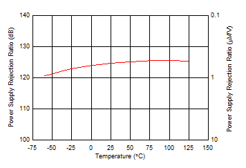
OPA1692 D012_SBOS566.gif
Figure 37. PSRR vs Temperature
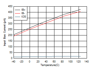
OPA1692 D016_SBOS566.gif
Figure 39. Input Bias and Offset Current vs Temperature
OPA1692 D006_SBOS566.gif
VS = ±1.75 V
Figure 41. IB vs Common-Mode Voltage
OPA1692 D008_SBOS566.gif
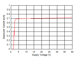
Figure 43. Supply Current vs Supply Voltage
OPA1692 D003_SBOS566.gif
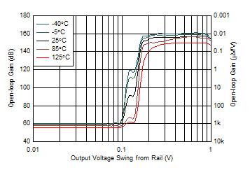
VS = ±1.75 V
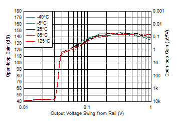
Figure 45. Open-Loop Gain vs Output Voltage
OPA1692 D011_SBOS566.gif
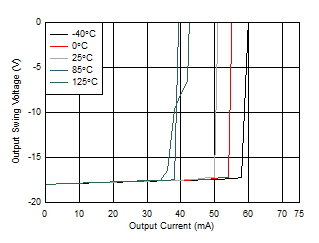
Sinking
Figure 47. Output Voltage vs Output Current
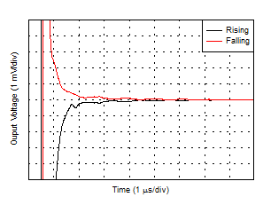
OPA1692 D033_SBOS566.gif
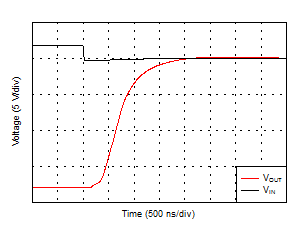
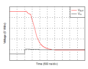
Figure 49. Negative Overload Recovery
OPA1692 D031_SBOS566.gif
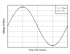
Figure 51. No Phase Reversal
OPA1692 D205_SBOS566.gif
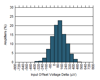
N = 580 Mean = 17 µV Std. Dev. = 145.2 µV
Figure 2. Input Offset Voltage Matching (Ch. A – Ch. B)
OPA1692 D206_SBOS566.gif
N = 1160 Mean = 301.5 nA Std. Dev. = 7.03 nA
Figure 4. Input Bias Current Distribution
OPA1692 D208_SBOS566.gif
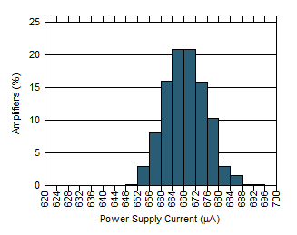
N = 1160 Mean = 664.6 µA Std. Dev. = 6.98 µA
Figure 6. Power Supply Current Distribution
OPA1692 D018_SBOS566.gif
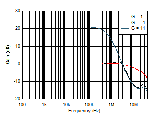
Figure 8. Closed-Loop Gain vs Frequency
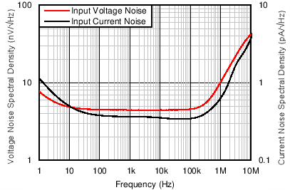
OPA1692 C006_SBOS566.png
Figure 10. Input Voltage Noise Spectral Density
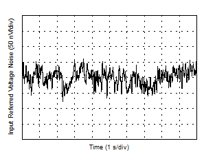
OPA1692 D041_SBOS566.gif
Figure 12. 0.1-Hz to 10-Hz Voltage Noise
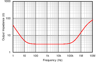
OPA1692 C005_SBOS566.png
Figure 14. Open-Loop Output Impedance vs Frequency
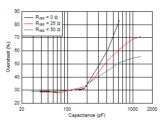
OPA1692 D038_SBOS566.gif
G = 1 10-mV input step
Figure 16. Overshoot vs Capacitive Load
OPA1692 D026_SBOS566.gif
VOUT = 3 VRMS 80-kHz bandwidth
Figure 18. THD + N Ratio vs Frequency
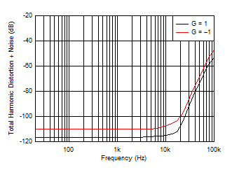
OPA1692 D027_SBOS566.gif
VOUT = 3 VRMS 500-kHz bandwidth
Figure 20. THD + N Ratio vs Frequency
OPA1692 D020_SBOS566.gif
VOUT = 3 VRMS G = –1 80-kHz bandwidth
Figure 22. Distortion Harmonics vs Frequency
OPA1692 D025_SBOS566.gif
f = 1 kHz RL = 600 Ω 80-kHz bandwidth
Figure 24. THD + N Ratio vs Output Amplitude
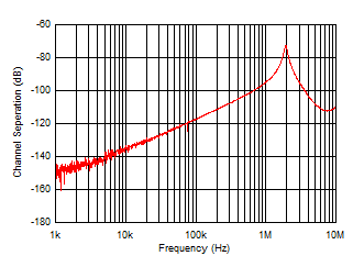
OPA1692 D029_SBOS566.gif
Figure 26. Channel Separation vs Frequency
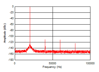
OPA1692 D203_SBOS901.gif
f = 20 kHz VO = 3 VRMS RL = 600 Ω
Figure 28. 20-kHz Output Spectrum
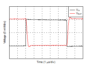
OPA1692 D037_SBOS566.gif
100-pF capacitive load 10-mV input step G = –1
Figure 30. Small-Signal Step Response
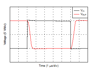
OPA1692 D035_SBOS566.gif
100-pF capacitive load 10-V input step G = –1
Figure 32. Large-Signal Step Response
OPA1692 D014_SBOS566.gif
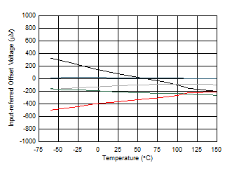
5 typical units
Figure 34. Input Offset Voltage vs Temperature
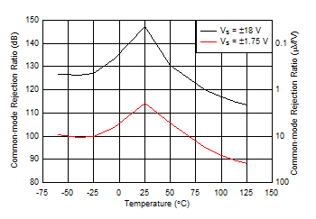
OPA1692 D004_SBOS566.gif
Figure 36. CMRR vs Temperature
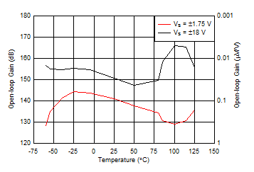
OPA1692 D001_SBOS566.gif
Figure 38. Open-Loop Gain vs Temperature
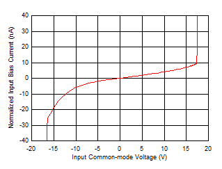
OPA1692 D005_SBOS566.gif
Figure 40. IB vs Common-Mode Voltage
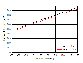
OPA1692 D007_SBOS566.gif
Figure 42. Supply Current vs Temperature
OPA1692 D002_SBOS566.gif
Figure 44. Open-Loop Gain vs Output Voltage
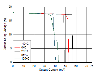
OPA1692 D010_SBOS566.gif
Sourcing
Figure 46. Output Voltage vs Output Current
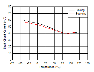
OPA1692 D009_SBOS566.gif
Figure 48. Short-Circuit Current vs Temperature
OPA1692 D032_SBOS566.gif
Figure 50. Positive Overload Recovery
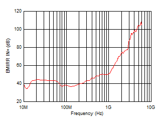
OPA1692 D030_SBOS566.gif
Figure 52. EMI Rejection Ratio (EMIRR)