ZHCSFP9B
December 2016 – November 2017
OPA170-Q1
,
OPA2170-Q1
,
OPA4170-Q1
PRODUCTION DATA.
1
特性
2
应用
3
说明
Device Images
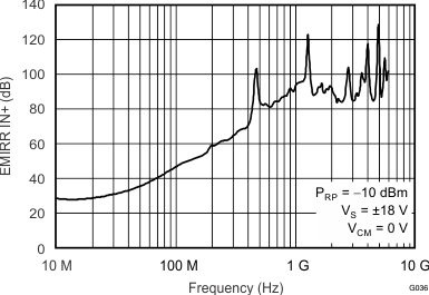
EMIRR IN+ 与频率间的关系
4
修订历史记录
5
Pin Configuration and Functions
Table 1.
Pin Functions: OPA170-Q1
Table 2.
Pin Functions: OPA2170-Q1
Table 3.
Pin Functions: OPA4170-Q1
6
Specifications
6.1
Absolute Maximum Ratings
6.2
ESD Ratings
6.3
Recommended Operating Conditions
6.4
Thermal Information: OPA170-Q1
6.5
Thermal Information: OPA2170-Q1
6.6
Thermal Information: OPA4170-Q1
6.7
Electrical Characteristics
6.8
Typical Characteristics: Table of Graphs
6.9
Typical Characteristics
7
Detailed Description
7.1
Overview
7.2
Functional Block Diagram
7.3
Feature Description
7.3.1
Operating Characteristics
7.3.2
Phase-Reversal Protection
7.3.3
Electrical Overstress
7.3.4
Capacitive Load and Stability
7.4
Device Functional Modes
7.4.1
Common-Mode Voltage Range
7.4.2
Overload Recovery
8
Application and Implementation
8.1
Application Information
8.2
Typical Application
8.2.1
Design Requirements
8.2.2
Detailed Design Procedure
8.2.3
Application Curve
9
Power Supply Recommendations
10
Layout
10.1
Layout Guidelines
10.2
Layout Example
11
器件和文档支持
11.1
器件支持
11.1.1
开发支持
11.1.1.1
TINA-TI™(免费软件下载)
11.1.1.2
DIP 适配器 EVM
11.1.1.3
通用运算放大器评估模块 (EVM)
11.1.1.4
TI 高精度设计
11.1.1.5
WEBENCH滤波器设计器
11.2
文档支持
11.2.1
相关文档
11.3
相关链接
11.4
社区资源
11.5
商标
11.6
静电放电警告
11.7
Glossary
12
机械、封装和可订购信息
封装选项
机械数据 (封装 | 引脚)
DBV|5
MPDS018T
散热焊盘机械数据 (封装 | 引脚)
订购信息
zhcsfp9b_oa
zhcsfp9b_pm
6.9
Typical Characteristics
V
S
= ±18 V, V
CM
= V
S
/ 2, R
LOAD
= 10 kΩ connected to V
S
/ 2, and C
L
= 100 pF (unless otherwise noted)
Figure 1.
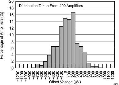
Offset Voltage Production Distribution
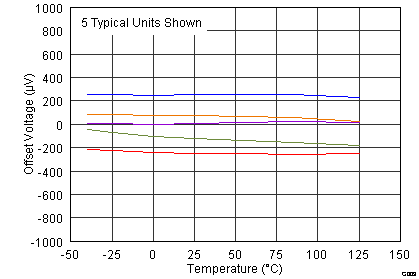
Figure 3.
Offset Voltage vs Temperature
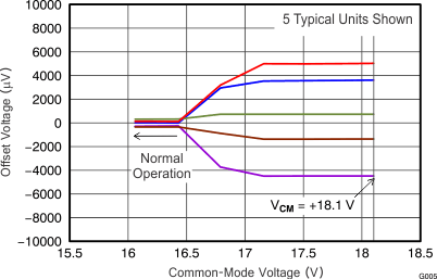
Figure 5.
Offset Voltage vs Common-Mode Voltage
(Upper Stage)
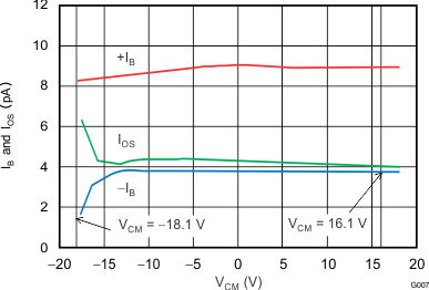
Figure 7.
I
B
and I
OS
vs Common-Mode Voltage
Figure 9.
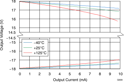
Output Voltage Swing vs Output Current (Maximum Supply)
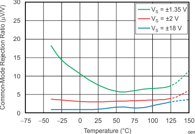
Figure 11.
CMRR vs Temperature
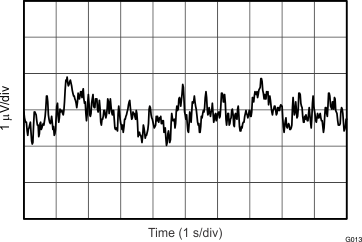
Figure 13.
0.1-Hz to 10-Hz Noise
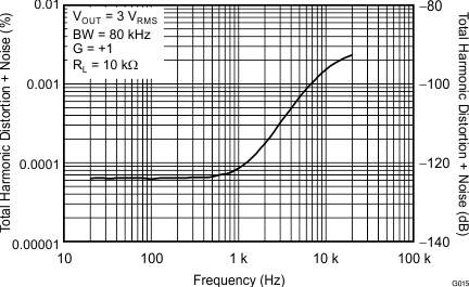
Figure 15.
THD + N Ratio vs Frequency
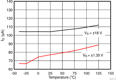
Figure 17.
Quiescent Current vs Temperature
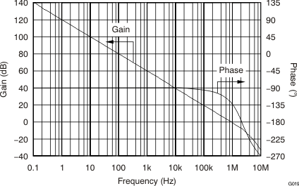
Figure 19.
Open-Loop Gain and Phase vs Frequency
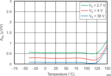
Figure 21.
Open-Loop Gain vs Temperature
100-mV output step
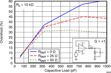
Figure 23.
Small-Signal Overshoot vs Capacitive Load
Figure 25.
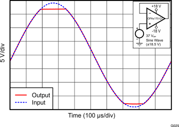
No Phase Reversal
Figure 27.
Negative Overload Recovery
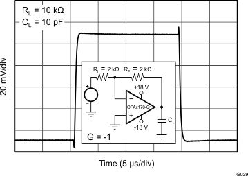
Figure 29.
Small-Signal Step Response (100-mV)
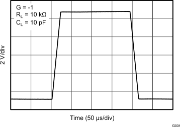
Figure 31.
Large-Signal Step Response
10-V negative step
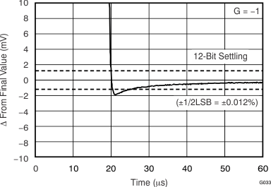
Figure 33.
Large-Signal Settling Time
Figure 35.
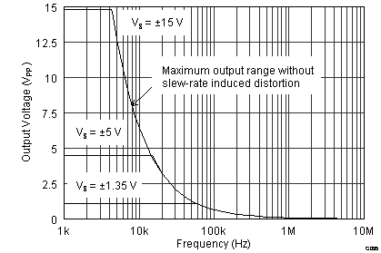
Maximum Output Voltage vs Frequency
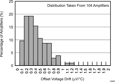
Figure 2.
Offset Voltage Drift Distribution
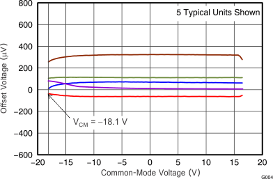
Figure 4.
Offset Voltage vs Common-Mode Voltage
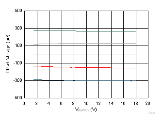
Figure 6.
Offset Voltage vs Power Supply
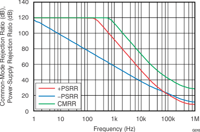
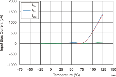
Figure 8.
Input Bias Current vs Temperature for Single and Dual Versions
Figure 10.
CMRR and PSRR vs Frequency
(Referred to Input)
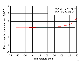
Figure 12.
PSRR vs Temperature
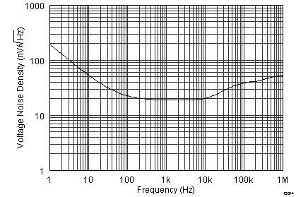
Figure 14.
Input Voltage Noise Spectral Density vs Frequency
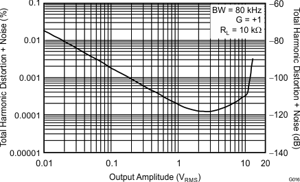
Figure 16.
THD + N vs Output Amplitude
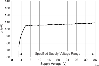
Figure 18.
Quiescent Current vs Supply Voltage
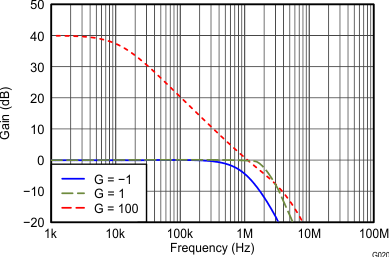
Figure 20.
Closed-Loop Gain vs Frequency
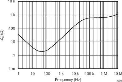
Figure 22.
Open-Loop Output Impedance vs Frequency
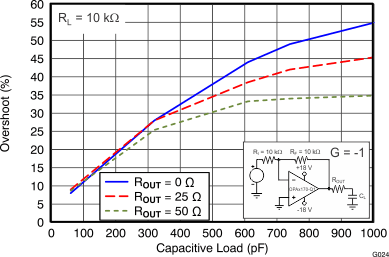
100-mV output step
Figure 24.
Small-Signal Overshoot vs Capacitive Load
Figure 26.
Positive Overload Recovery
Figure 28.
Small-Signal Step Response (100-mV)
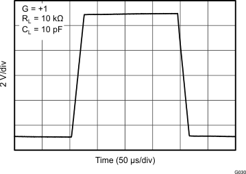
Figure 30.
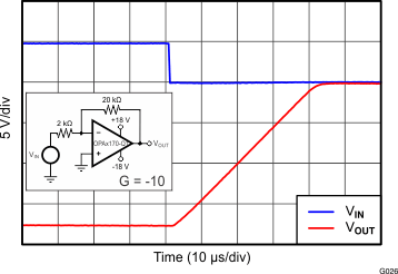
Large-Signal Step Response
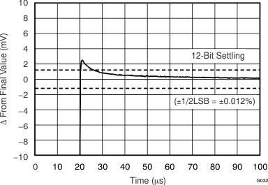
10-V positive step
Figure 32.
Large-Signal Settling Time
10-V negative step
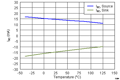
Figure 34.
Short-Circuit Current vs Temperature
Figure 36.
EMIRR IN+ vs Frequency
千亿体育app官网登录(中国)官方网站IOS/安卓通用版/手机APP
|
米乐app下载官网(中国)|ios|Android/通用版APP最新版
|
米乐|米乐·M6(中国大陆)官方网站
|
千亿体育登陆地址
|
华体会体育(中国)HTH·官方网站
|
千赢qy国际_全站最新版千赢qy国际V6.2.14安卓/IOS下载
|
18新利网v1.2.5|中国官方网站
|
bob电竞真人(中国官网)安卓/ios苹果/电脑版【1.97.95版下载】
|
千亿体育app官方下载(中国)官方网站IOS/安卓/手机APP下载安装
|