ZHCSBX8I December 2013 – May 2018 OPA172 , OPA2172 , OPA4172
PRODUCTION DATA.
- 1 特性
- 2 应用
- 3 说明
- 4 修订历史记录
- 5 Device Comparison
- 6 Pin Configuration and Functions
- 7 Specifications
- 8 Detailed Description
- 9 Applications and Implementation
- 10Power-Supply Recommendations
- 11Layout
- 12器件和文档支持
- 13机械、封装和可订购信息
封装选项
机械数据 (封装 | 引脚)
散热焊盘机械数据 (封装 | 引脚)
订购信息
9.2.3 JFET-Input Low-Noise Amplifier
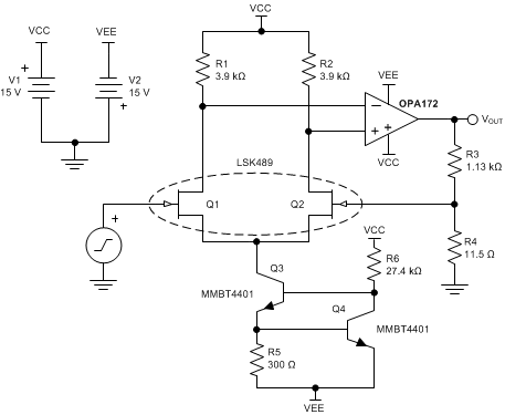
Figure 51 shows a low-noise composite amplifier built by adding a low noise JFET pair (Q1 and Q2) as an input preamplifier for the OPA172. Transistors Q3 and Q4 form a 2-mA current sink that biases each JFET with 1 mA of drain current. Using 3.9-kΩ drain resistors produces a gain of approximately 10 in the input amplifier, making the extremely-low, broadband-noise spectral density of the JFET pair, Q1 and Q2, the dominant noise source of the amplifier. The output impedance of the input differential amplifier is large enough that a FET-input amplifier such as the OPA172 provides superior noise performance over bipolar-input amplifiers.
The gain of the composite amplifier is given by Equation 3:
The resistances shown are standard 1% resistor values that produce a gain of approximately 100 (99.26) with 68° of phase margin. Gains less than 10 may require additional compensation methods to provide stability. Select low resistor values to minimize the resistor thermal noise contribution to the total output noise.
 Figure 51. JFET-Input Low-Noise Amplifier