ZHCSSH3A September   2000  – September 2023 OPA177

PRODUCTION DATA  

  1.   1
  2. 1特性
  3. 2应用
  4. 3说明
  5. 4Revision History
  6. 5Pin Configuration and Functions
  7. 6Specifications
    1. 6.1 Absolute Maximum Ratings
    2. 6.2 ESD Ratings
    3. 6.3 Recommended Operating Conditions
    4. 6.4 Thermal Information
    5. 6.5 Electrical Characteristics
    6. 6.6 Typical Characteristics
  8. 7Application and Implementation
    1. 7.1 Application Information
      1. 7.1.1 Offset Voltage Adjustment
      2. 7.1.2 Input Protection
      3. 7.1.3 Noise Performance
      4. 7.1.4 Input Bias Current Cancellation
    2. 7.2 Typical Application
  9. 8Device and Documentation Support
    1. 8.1 器件支持
      1. 8.1.1 开发支持
        1. 8.1.1.1 PSpice® for TI
        2. 8.1.1.2 TINA-TI™ 仿真软件(免费下载)
        3. 8.1.1.3 DIP-Adapter-EVM
        4. 8.1.1.4 DIYAMP-EVM
        5. 8.1.1.5 TI 参考设计
        6. 8.1.1.6 滤波器设计工具
    2. 8.2 接收文档更新通知
    3. 8.3 支持资源
    4. 8.4 Trademarks
    5. 8.5 静电放电警告
    6. 8.6 术语表
  10. 9Mechanical, Packaging, and Orderable Information

封装选项

请参考 PDF 数据表获取器件具体的封装图。

机械数据 (封装 | 引脚)
  • D|8
  • P|8
散热焊盘机械数据 (封装 | 引脚)
订购信息

Pin Configuration and Functions

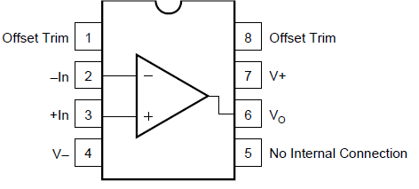
GUID-20211112-SS0I-QWVN-ZTXK-DCGHVMLDMGD0-low.png Figure 5-1 D Package, 8-Pin SOIC
and P Package, 8-Pin PDIP
(Top View)
Table 5-1 Pin Functions
PIN TYPE DESCRIPTION
NAME NO.
+In 3 Input Noninverting input
−In 2 Input Inverting input
No Internal Connection 5 No internal connection (can be left floating)
Offset Trim 1, 8 Input offset voltage trim (leave floating if not used)
V+ 7 Power Positive (highest) power supply
V− 4 Power Negative (lowest) power supply
VO 6 Output Output