SBOS850 December 2017 OPA192-Q1 , OPA2192-Q1
PRODUCTION DATA.
- 1 Features
- 2 Applications
- 3 Description
- 4 Revision History
- 5 Pin Configuration and Functions
-
6 Specifications
- 6.1 Absolute Maximum Ratings
- 6.2 ESD Ratings
- 6.3 Recommended Operating Conditions
- 6.4 Thermal Information: OPA192-Q1
- 6.5 Thermal Information: OPA2192-Q1
- 6.6 Electrical Characteristics: VS = ±4 V to ±18 V (VS = 8 V to 36 V)
- 6.7 Electrical Characteristics: VS = ±2.25 V to ±4 V (VS = 4.5 V to 8 V)
- 6.8 Typical Characteristics
- 6.9 Typical Characteristics
- 7 Parameter Measurement Information
- 8 Detailed Description
- 9 Application and Implementation
- 10Power-Supply Recommendations
- 11Layout
- 12Device and Documentation Support
- 13Mechanical, Packaging, and Orderable Information
8 Detailed Description
8.1 Overview
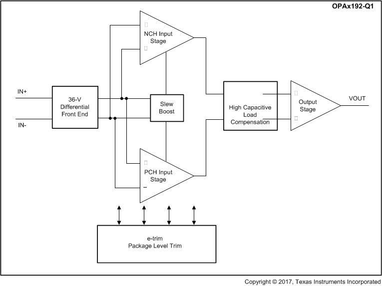
The OPAx192-Q1 family of operational amplifiers use e-trim, a method of package-level trim for offset and offset temperature drift implemented during the final steps of manufacturing after the plastic molding process. This method minimizes the influence of inherent input transistor mismatch, as well as errors induced during package molding. The trim communication occurs on the output pin of the standard pinout, and after the trim points are set, further communication to the trim structure is permanently disabled. The Functional Block Diagram shows the simplified diagram of the OPAx192-Q1 with e-trim.
Unlike previous e-trim op amps, the OPAx192-Q1 uses a patented two-temperature trim architecture to achieve a very low offset voltage of 25 µV (maximum) and low voltage offset drift of 0.5 µV/°C (maximum) over the full specified temperature range. This level of precision performance at wide supply voltages makes these amplifiers useful for high-impedance industrial sensors, filters, and high-voltage data acquisition.
8.2 Functional Block Diagram
8.3 Feature Description
8.3.1 Input Protection Circuitry
The OPAx192-Q1 uses a unique input architecture to eliminate the need for input protection diodes but still provides robust input protection under transient conditions. Conventional input diode protection schemes shown in Figure 49 can be activated by fast transient step responses and can introduce signal distortion and settling time delays because of alternate current paths, as shown in Figure 50. For low-gain circuits, these fast-ramping input signals forward-bias back-to-back diodes, causing an increase in input current, and resulting in extended settling time, as shown in Figure 51.
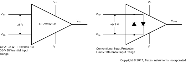 Figure 49. OPAx192-Q1 Input Protection Does Not Limit Differential Input Capability
 Figure 50. Back-to-Back Diodes Create Settling Issues
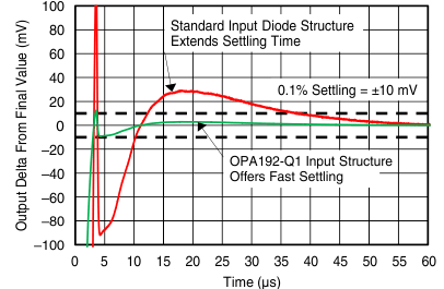 Figure 51. OPAx192-Q1 Protection Circuit Maintains Fast-Settling Transient Response
The OPAx192-Q1 family of operational amplifiers provides a true high-impedance differential input capability for high-voltage applications. This patented input protection architecture does not introduce additional signal distortion or delayed settling time, making the device an optimal op amp for multichannel, high-switched, input applications. The OPAx192-Q1 can tolerate a maximum differential swing (voltage between inverting and noninverting pins of the op amp) of up to 36 V, making the device suitable for use as a comparator or in applications with fast-ramping input signals such as multiplexed data-acquisition systems; see Figure 61.
8.3.2 EMI Rejection
The OPAx192-Q1 uses integrated electromagnetic interference (EMI) filtering to reduce the effects of EMI from sources such as wireless communications and densely-populated boards with a mix of analog signal chain and digital components. EMI immunity can be improved with circuit design techniques; the OPAx192-Q1 benefits from these design improvements. Texas Instruments has developed the ability to accurately measure and quantify the immunity of an operational amplifier over a broad frequency spectrum extending from 10 MHz
to 6 GHz. Figure 52 shows the results of this testing on the OPAx192-Q1. Table 2 shows the EMIRR IN+ values for the OPAx192-Q1 at particular frequencies commonly encountered in real-world applications. Applications listed in Table 2 may be centered on or operated near the particular frequency shown. Detailed information can also be found in the application report EMI Rejection Ratio of Operational Amplifiers available for download from www.ti.com.
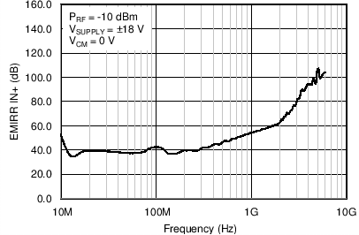 Figure 52. EMIRR Testing
Table 2. OPAx192-Q1 EMIRR IN+ For Frequencies of Interest
| FREQUENCY | APPLICATION OR ALLOCATION | EMIRR IN+ |
|---|---|---|
| 400 MHz | Mobile radio, mobile satellite, space operation, weather, radar, ultra-high frequency (UHF) applications | 44.1 dB |
| 900 MHz | Global system for mobile communications (GSM) applications, radio communication, navigation, GPS (to 1.6 GHz), GSM, aeronautical mobile, UHF applications | 52.8 dB |
| 1.8 GHz | GSM applications, mobile personal communications, broadband, satellite, L-band (1 GHz to 2 GHz) | 61.0 dB |
| 2.4 GHz | 802.11b, 802.11g, 802.11n, Bluetooth®, mobile personal communications, industrial, scientific and medical (ISM) radio band, amateur radio and satellite, S-band (2 GHz to 4 GHz) | 69.5 dB |
| 3.6 GHz | Radiolocation, aero communication and navigation, satellite, mobile, S-band | 88.7 dB |
| 5 GHz | 802.11a, 802.11n, aero communication and navigation, mobile communication, space and satellite operation, C-band (4 GHz to 8 GHz) | 105.5 dB |
8.3.3 Phase Reversal Protection
The OPAx192-Q1 family has internal phase-reversal protection. Many op amps exhibit a phase reversal when the input is driven beyond its linear common-mode range. This condition is most often encountered in noninverting circuits when the input is driven beyond the specified common-mode voltage range, causing the output to reverse into the opposite rail. The OPAx192-Q1 is a rail-to-rail input op amp; therefore, the common-mode range can extend up to the rails. Input signals beyond the rails do not cause phase reversal; instead, the output limits into the appropriate rail. This performance is shown in Figure 53.
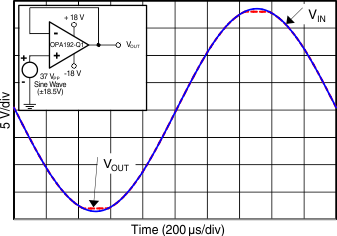 Figure 53. No Phase Reversal
8.3.4 Thermal Protection
The internal power dissipation of any amplifier causes its internal (junction) temperature to rise. This phenomenon is called self heating. The absolute maximum junction temperature of the OPAx192-Q1 is 150°C. Exceeding this temperature causes damage to the device. The OPAx192-Q1 has a thermal protection feature that prevents damage from self heating. The protection works by monitoring the temperature of the device and turning off the op amp output drive for temperatures above 140°C. Figure 54 shows an application example for the OPAx192-Q1 that has significant self heating (159°C) because of the power dissipation (0.81 W). Thermal calculations indicate that for an ambient temperature of 65°C the device junction temperature must reach 187°C. The actual device, however, turns off the output drive to maintain a safe junction temperature. Figure 54 shows how the circuit behaves during thermal protection. During normal operation, the device acts as a buffer so the output is 3 V. When self heating causes the device junction temperature to increase above 140°C, the thermal protection forces the output to a high-impedance state and the output is pulled to ground through resistor RL.
 Figure 54. Thermal Protection
8.3.5 Capacitive Load and Stability
The OPAx192-Q1 features a patented output stage capable of driving large capacitive loads, and in a unity-gain configuration, directly drives up to 1 nF of pure capacitive load. Increasing the gain enhances the ability of the amplifier to drive greater capacitive loads; see Figure 55 and Figure 56. The particular op amp circuit configuration, layout, gain, and output loading are some of the factors to consider when establishing whether an amplifier is stable in operation.
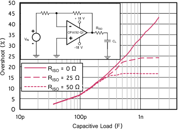 Figure 55. Small-Signal Overshoot vs Capacitive Load (100-mV Output Step)
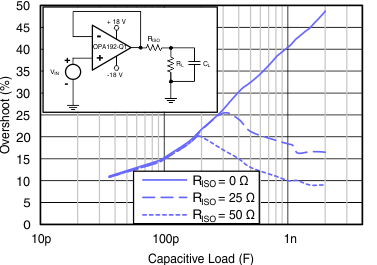 Figure 56. Small-Signal Overshoot vs Capacitive Load (100-mV Output Step)
For additional drive capability in unity-gain configurations, improve capacitive load drive by inserting a small
(10 Ω to 20 Ω) resistor, RISO, in series with the output, as shown in Figure 57. This resistor significantly reduces ringing and maintains dc performance for purely capacitive loads. However, if a resistive load is in parallel with the capacitive load, then a voltage divider is created, thus introducing a gain error at the output and slightly reducing the output swing. The error introduced is proportional to the ratio RISO / RL, and is generally negligible at low output levels. A high capacitive-load drive makes the OPAx192-Q1 work well with applications such as reference buffers, MOSFET gate drives, and cable-shield drives. The circuit shown in Figure 57 uses an isolation resistor, RISO, to stabilize the output of an op amp. RISO modifies the open-loop gain of the system for increased phase margin, and results using the OPAx192-Q1 are summarized in Table 3. For additional information on techniques to optimize and design using this circuit, TI Precision Design Capacitive Load Drive Solution using an Isolation Resistor details complete design goals, simulation, and test results.
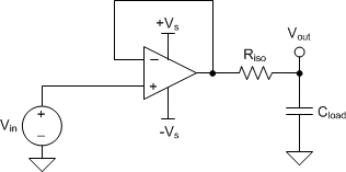 Figure 57. Extending Capacitive Load Drive with the OPAx192-Q1
Table 3. OPAx192-Q1 Capacitive Load Drive Solution Using Isolation Resistor Comparison of Calculated and Measured Results
| PARAMETER | VALUE | |||||||||
|---|---|---|---|---|---|---|---|---|---|---|
| Capacitive Load | 100 pF | 1000 pF | 0.01 µF | 0.1 µF | 1 µF | |||||
| Phase Margin | 45° | 60° | 45° | 60° | 45° | 60° | 45° | 60° | 45° | 60° |
| RISO (Ω) | 47 | 360 | 24 | 100 | 20 | 51 | 6.2 | 15.8 | 2 | 4.7 |
| Measured Overshoot (%) | 23.2 8.6 | 10.4 | 22.5 | 9.0 | 22.1 | 8.7 | 23.1 | 8.6 | 21 | 8.6 |
| Calculated PM | 45.1° | 58.1° | 45.8° | 59.7° | 46.1° | 60.1° | 45.2° | 60.2° | 47.2° | 60.2° |
 |
For step-by-step design procedure, circuit schematics, bill of materials, printed circuit board (PCB) files, simulation results, and test results, refer to TI Precision Design TIDU032, Capacitive Load Drive Solution using an Isolation Resistor . |
8.3.6 Common-Mode Voltage Range
The OPAx192-Q1 is a 36-V, true rail-to-rail input operational amplifier with an input common-mode range that extends 100 mV beyond either supply rail. This wide range is achieved with paralleled complementary N-channel and P-channel differential input pairs, as shown in Figure 58. The N-channel pair is active for input voltages close to the positive rail, typically (V+) – 3 V to 100 mV above the positive supply. The P-channel pair is active for inputs from 100 mV below the negative supply to approximately (V+) – 1.5 V. There is a small transition region, typically (V+) –3 V to (V+) – 1.5 V in which both input pairs are on. This transition region can vary modestly with process variation, and within this region PSRR, CMRR, offset voltage, offset drift, noise and THD performance may be degraded compared to operation outside this region.
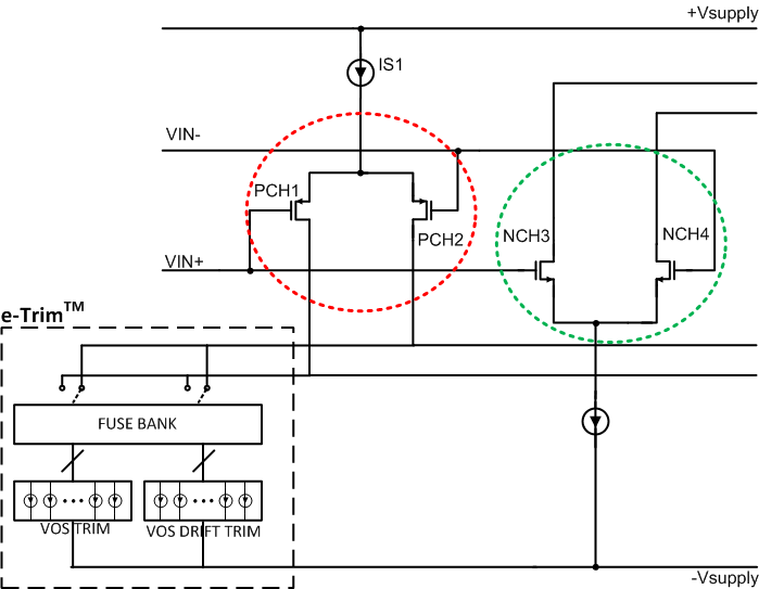 Figure 58. Rail-to-Rail Input Stage
To achieve the best performance for two-stage rail-to-rail input amplifiers, avoid the transition region when possible. The OPAx192-Q1 uses a precision trim for both the N-channel and P-channel regions. This technique enables significantly lower levels of offset than previous-generation devices, causing variance in the transition region of the input stages to appear exaggerated relative to offset over the full common-mode range, as shown in Figure 59.
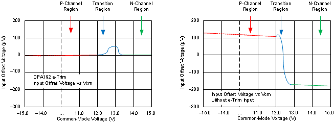 Figure 59. Common-Mode Transition vs Standard Rail-to-Rail Amplifiers
8.3.7 Electrical Overstress
Designers often ask questions about the capability of an operational amplifier to withstand electrical overstress (EOS). These questions tend to focus on the device inputs, but may involve the supply voltage pins or even the output pin. Each of these different pin functions have electrical stress limits determined by the voltage breakdown characteristics of the particular semiconductor fabrication process and specific circuits connected to the pin. Additionally, internal electrostatic discharge (ESD) protection is built into these circuits to protect them from accidental ESD events both before and during product assembly.
Having a good understanding of this basic ESD circuitry and its relevance to an electrical overstress event is helpful. Figure 60 shows an illustration of the ESD circuits contained in the OPAx192-Q1 (indicated by the dashed line area). The ESD protection circuitry involves several current-steering diodes connected from the input and output pins and routed back to the internal power-supply lines, where the diodes meet at an absorption device or the power-supply ESD cell, internal to the operational amplifier. This protection circuitry is intended to remain inactive during normal circuit operation.
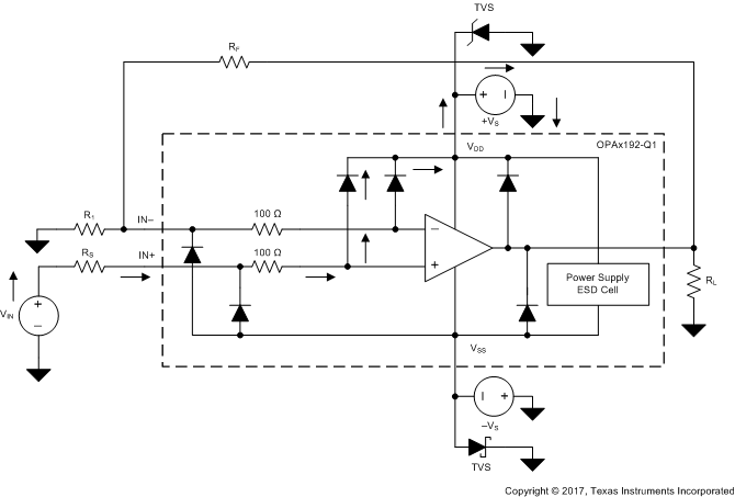 Figure 60. Equivalent Internal ESD Circuitry Relative to a Typical Circuit Application
An ESD event is very short in duration and very high voltage (for example, 1 kV, 100 ns), whereas an EOS event is long duration and lower voltage (for example, 50 V, 100 ms). The ESD diodes are designed for out-of-circuit ESD protection (that is, during assembly, test, and storage of the device before being soldered to the PCB). During an ESD event, the ESD signal is passed through the ESD steering diodes to an absorption circuit (labeled ESD power-supply circuit). The ESD absorption circuit clamps the supplies to a safe level.
Although this behavior is necessary for out-of-circuit protection, excessive current and damage is caused if activated in-circuit. A transient voltage suppressors (TVS) can be used to prevent against damage caused by turning on the ESD absorption circuit during an in-circuit ESD event. Using the appropriate current limiting resistors and TVS diodes allows for the use of device ESD diodes to protect against EOS events.
8.3.8 Overload Recovery
Overload recovery is defined as the time required for the op amp output to recover from a saturated state to a linear state. The output devices of the op amp enter a saturation region when the output voltage exceeds the rated operating voltage, either due to the high input voltage or the high gain. After the device enters the saturation region, the charge carriers in the output devices require time to return back to the linear state. After the charge carriers return back to the linear state, the device begins to slew at the specified slew rate. Thus, the propagation delay in case of an overload condition is the sum of the overload recovery time and the slew time. The overload recovery time for the OPAx192-Q1 is approximately 200 ns.
8.4 Device Functional Modes
The OPAx192-Q1 has a single functional mode and is operational when the power-supply voltage is greater than
4.5 V (±2.25 V). The maximum power supply voltage for the OPAx192-Q1 is 36 V (±18 V).