ZHCSHU3A March 2018 – January 2021 OPA197-Q1 , OPA2197-Q1 , OPA4197-Q1
PRODUCTION DATA
- 1 特性
- 2 应用
- 3 说明
- 4 Revision History
- 5 Pin Configuration and Functions
-
6 Specifications
- 6.1 Absolute Maximum Ratings
- 6.2 ESD Ratings
- 6.3 Recommended Operating Conditions
- 6.4 Thermal Information: OPA197-Q1
- 6.5 Thermal Information: OPA2197-Q1
- 6.6 Thermal Information: OPA4197-Q1
- 6.7 Electrical Characteristics: VS = ±4 V to ±18 V (VS = 8 V to 36 V)
- 6.8 Electrical Characteristics: VS = ±2.25 V to ±4 V (VS = 4.5 V to 8 V)
- 6.9 Typical Characteristics
- 7 Detailed Description
- 8 Application and Implementation
- 9 Power Supply Recommendations
- 10Layout
- 11Device and Documentation Support
- 12Mechanical, Packaging, and Orderable Information
7.3.5 Capacitive Load and Stability
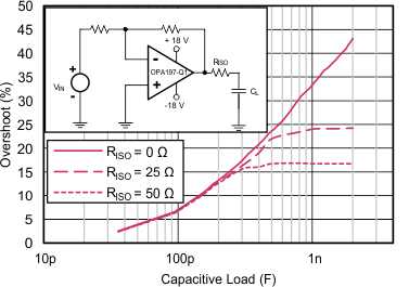
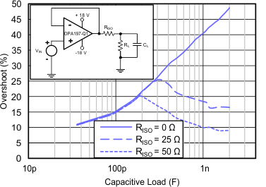
The OPAx197-Q1 feature a patented output stage capable of driving large capacitive loads, and in a unity-gain configuration, directly drive up to 1 nF of pure capacitive load. Increasing the gain enhances the ability of these amplifiers to drive greater capacitive loads; see Figure 7-7 and Figure 7-8. The particular op-amp circuit configuration, layout, gain, and output loading are some of the factors to consider when establishing whether an amplifier is stable in operation.
 Figure 7-7 Small-Signal Overshoot vs Capacitive Load (100-mV Output Step)
 Figure 7-8 Small-Signal Overshoot vs Capacitive Load (100-mV Output Step)
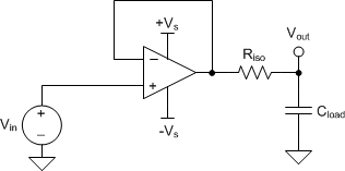
For additional drive capability in unity-gain configurations, improve capacitive load drive by inserting a small (10-Ω to 20-Ω) resistor, RISO, in series with the output, as shown in Figure 7-9. This resistor significantly reduces ringing and maintains dc performance for purely capacitive loads. However, if a resistive load is in parallel with the capacitive load, then a voltage divider is created, thus introducing a gain error at the output and slightly reducing the output swing. The error introduced is proportional to the ratio RISO / RL, and is generally negligible at low output levels. A high capacitive load drive makes the OPAx197-Q1 a great choice for applications such as reference buffers, MOSFET gate drives, and cable-shield drives. The circuit shown in Figure 7-9 uses an isolation resistor, RISO, to stabilize the output of an op amp. RISO modifies the open-loop gain of the system for increased phase margin, and results using the OPAx197-Q1 are summarized in Table 7-2. For additional information on techniques to optimize and design using this circuit, TI Precision Design TIPD128 details complete design goals, simulation, and test results.
 Figure 7-9 Extending Capacitive Load
Drive With the OPAx197-Q1
Figure 7-9 Extending Capacitive Load
Drive With the OPAx197-Q1| PARAMETER | VALUE | |||||||||
|---|---|---|---|---|---|---|---|---|---|---|
| Capacitive Load | 100 pF | 1000 pF | 0.01 µF | 0.1 µF | 1 µF | |||||
| Phase Margin | 45° | 60° | 45° | 60° | 45° | 60° | 45° | 60° | 45° | 60° |
| RISO (Ω) | 47 | 360 | 24 | 100 | 20 | 51 | 6.2 | 15.8 | 2 | 4.7 |
| Measured Overshoot (%) | 23.2 8.6 | 10.4 | 22.5 | 9 | 22.1 | 8.7 | 23.1 | 8.6 | 21 | 8.6 |
| Calculated PM | 45.1° | 58.1° | 45.8° | 59.7° | 46.1° | 60.1° | 45.2° | 60.2° | 47.2° | 60.2° |
| For step-by-step design procedure, circuit schematics, bill of materials, printed circuit board (PCB) files, simulation results, and test results, see TI Precision Design TIPD128Capacitive Load Drive Solution using an Isolation Resistor. | |