SBOS426D November 2008 – October 2016 OPA209 , OPA2209 , OPA4209
PRODUCTION DATA.
- 1 Features
- 2 Applications
- 3 Description
- 4 Revision History
- 5 Pin Configuration and Functions
- 6 Specifications
- 7 Detailed Description
- 8 Application and Implementation
- 9 Power Supply Recommendations
- 10Layout
- 11Device and Documentation Support
- 12Mechanical, Packaging, and Orderable Information
封装选项
机械数据 (封装 | 引脚)
散热焊盘机械数据 (封装 | 引脚)
订购信息
8 Application and Implementation
NOTE
Information in the following applications sections is not part of the TI component specification, and TI does not warrant its accuracy or completeness. TI’s customers are responsible for determining suitability of components for their purposes. Customers should validate and test their design implementation to confirm system functionality.
8.1 Application Information
The OPAx209 are unity-gain stable, precision operational amplifiers with very low noise. Applications with noisy or high-impedance power supplies require decoupling capacitors close to the device pins. In most cases, 0.1-µF capacitors are adequate.
8.2 Typical Application
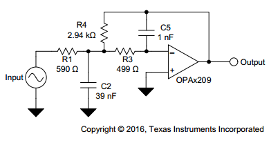
 Figure 35. Low-Pass Filter
8.2.1 Design Requirements
Low-pass filters are commonly employed in signal processing applications to reduce noise and prevent aliasing. The OPAx209 are ideally suited to construct high-speed, high-precision active filters. Figure 35 shows a second-order, low-pass filter commonly encountered in signal processing applications.
Use the following parameters for this design example:
- Gain = 5 V/V (inverting gain)
- Low-pass cutoff frequency = 25 kHz
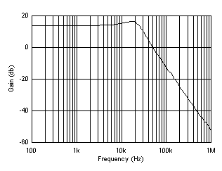
- Second-order Chebyshev filter response with 3-dB gain peaking in the passband
8.2.2 Detailed Design Procedure
The infinite-gain multiple-feedback circuit for a low-pass network function is shown in Figure 35. Use Equation 1 to calculate the voltage transfer function.

This circuit produces a signal inversion. For this circuit, the gain at DC and the low-pass cutoff frequency are calculated by Equation 2:

8.2.3 Application Curve
 Figure 36. OPAx209 Second-Order, 25-kHz, Chebyshev, Low-Pass Filter