ZHCSGC1F June   2017  – March 2021 OPA145 , OPA2145

PRODUCTION DATA  

  1. 特性
  2. 应用
  3. 说明
  4. Revision History
  5. Pin Configuration and Functions
  6. Specifications
    1. 6.1 Absolute Maximum Ratings
    2. 6.2 ESD Ratings
    3. 6.3 Recommended Operating Conditions
    4. 6.4 Thermal Information: OPA145
    5. 6.5 Thermal Information: OPA2145
    6. 6.6 Electrical Characteristics: VS = 4.5 V to 36 V; ±2.25 V to ±18 V
    7. 6.7 Typical Characteristics
  7. Detailed Description
    1. 7.1 Overview
    2. 7.2 Functional Block Diagram
    3. 7.3 Feature Description
      1. 7.3.1 Capacitive Load and Stability
      2. 7.3.2 Output Current Limit
      3. 7.3.3 Noise Performance
      4. 7.3.4 Basic Noise Calculations
      5. 7.3.5 Phase-Reversal Protection
      6. 7.3.6 Electrical Overstress
      7. 7.3.7 EMI Rejection
      8. 7.3.8 EMIRR +IN Test Configuration
    4. 7.4 Device Functional Modes
  8. Application and Implementation
    1. 8.1 Application Information
    2. 8.2 Typical Application
      1. 8.2.1 Design Requirements
      2. 8.2.2 Detailed Design Procedure
      3. 8.2.3 Application Curve
    3. 8.3 System Examples
      1. 8.3.1 16-Bit, 100-kSPS, Fully Differential Transimpedance Imaging and Measurement
  9. Power Supply Recommendations
  10. 10Layout
    1. 10.1 Layout Guidelines
    2. 10.2 Layout Example
  11. 11Device and Documentation Support
    1. 11.1 Device Support
      1. 11.1.1 Development Support
        1. 11.1.1.1 TINA-TI™ SImulation Software (Free Download)
        2. 11.1.1.2 WEBENCH Filter Designer Tool
        3. 11.1.1.3 TI Precision Designs
    2. 11.2 Documentation Support
      1. 11.2.1 Related Documentation
    3. 11.3 Receiving Notification of Documentation Updates
    4. 11.4 支持资源
    5. 11.5 Trademarks
    6. 11.6 静电放电警告
    7. 11.7 术语表
  12. 12Mechanical, Packaging, and Orderable Information

封装选项

机械数据 (封装 | 引脚)
散热焊盘机械数据 (封装 | 引脚)
订购信息

Typical Characteristics

at TA = 25°C, VS = ±18 V, VCM = VS / 2, RLOAD = 10 kΩ connected to VS / 2, and CL = 100 pF (unless otherwise noted)

Table 6-1 Table of Graphs
DESCRIPTION FIGURE
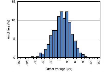
Offset Voltage Production Distribution Figure 6-1
Offset Voltage Drift Distribution From –40°C to +125°C Figure 6-2
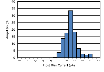
Input Bias Current Production Distribution Figure 6-3
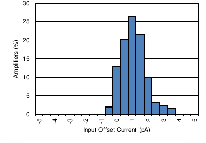
Input Offset Current Production Distribution Figure 6-4
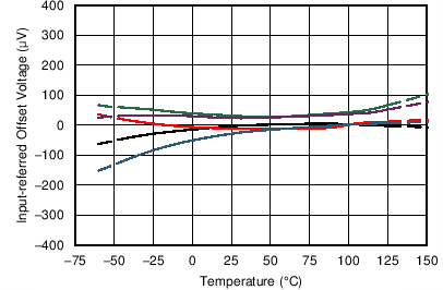
Offset Voltage vs Temperature Figure 6-5
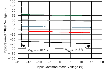
Offset Voltage vs Common-Mode Voltage Figure 6-6
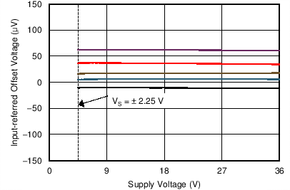
Offset Voltage vs Power Supply Figure 6-7
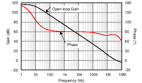
Open-Loop Gain and Phase vs Frequency Figure 6-8
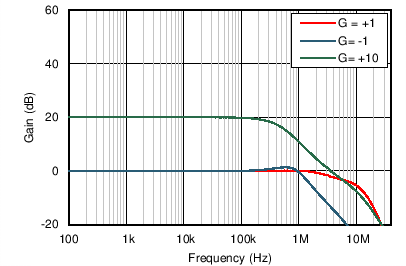
Closed-Loop Gain vs Frequency Figure 6-9
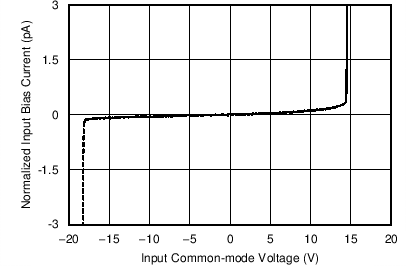
Input Bias Current vs Common-Mode Voltage Figure 6-10
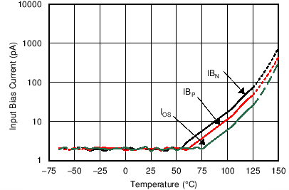
Input Bias Current and Offset vs Temperature Figure 6-11
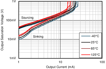
Output Voltage Swing vs Output Current (Maximum Supply) Figure 6-12
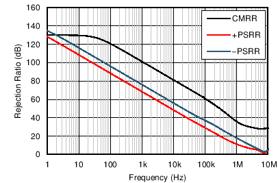
CMRR and PSRR vs Frequency Figure 6-13
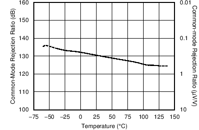
CMRR vs Temperature Figure 6-14
PSRR vs Temperature Figure 6-15
0.1-Hz to 10-Hz Voltage Noise Figure 6-16
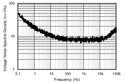
Input Voltage Noise Spectral Density vs Frequency Figure 6-17
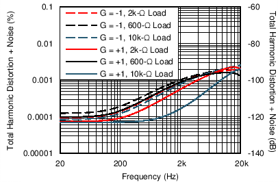
THD+N Ratio vs Frequency Figure 6-18
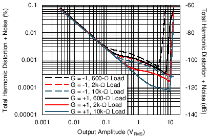
THD+N vs Output Amplitude Figure 6-19
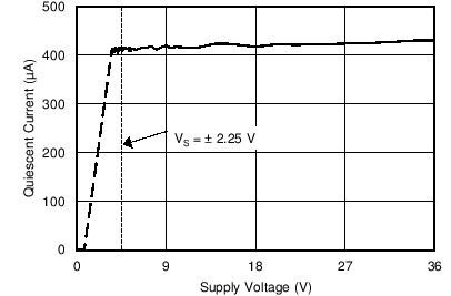
Quiescent Current vs Supply Voltage Figure 6-20
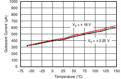
Quiescent Current vs Temperature Figure 6-21
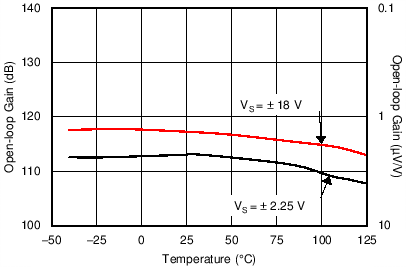
Open-Loop Gain vs Temperature (10-kΩ) Figure 6-22
Open-Loop Gain vs Temperature (2-kΩ) Figure 6-23
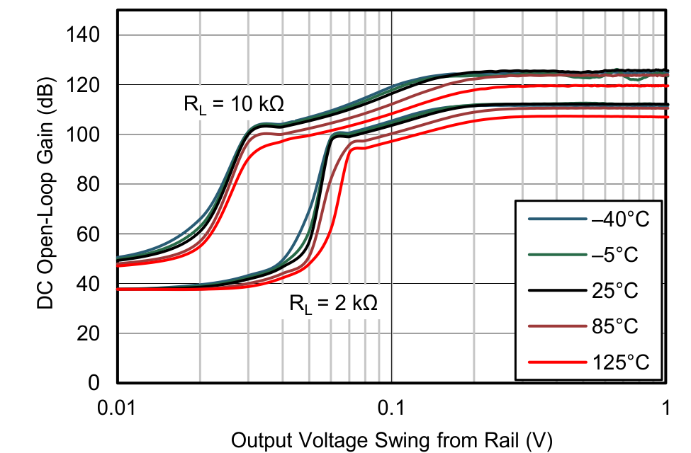
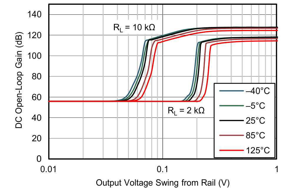
DC Open-Loop Gain vs Output Voltage Swing Relative to Supply Figure 6-24, Figure 6-25
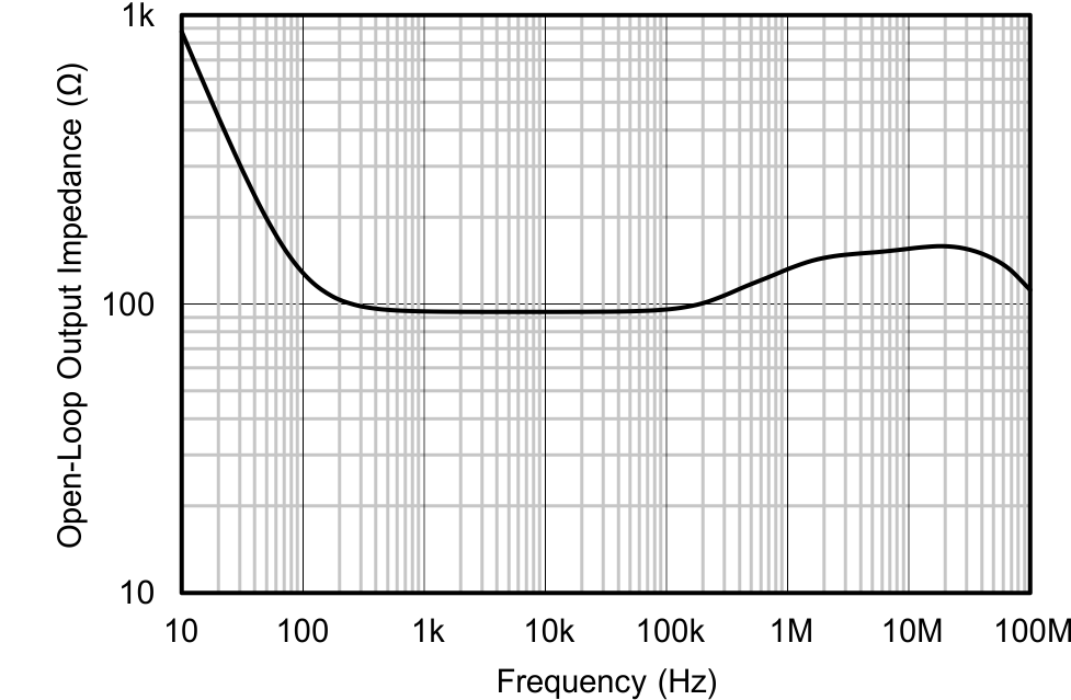
Open-Loop Output Impedance vs Frequency Figure 6-26
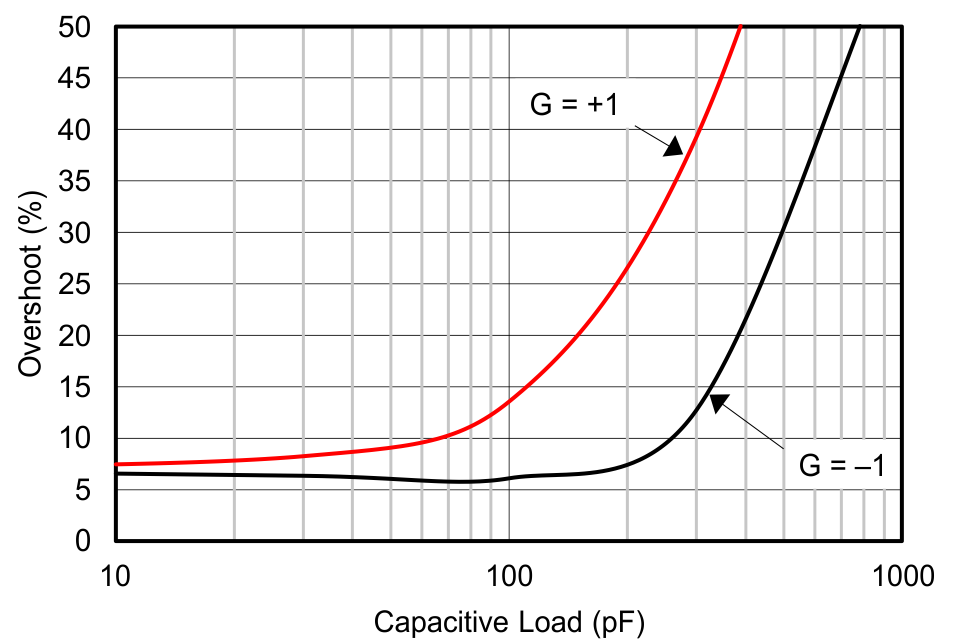
Small-Signal Overshoot vs Capacitive Load (10-mV Step) Figure 6-27
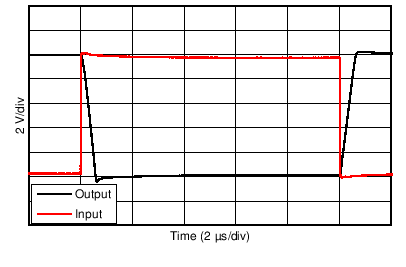
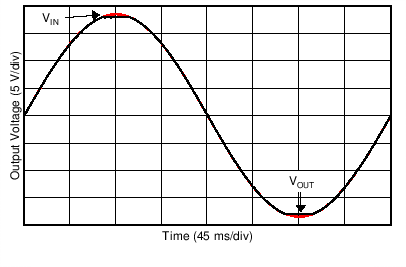
No Phase Reversal Figure 6-28
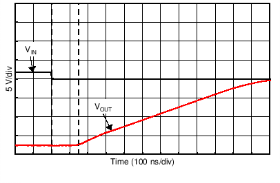
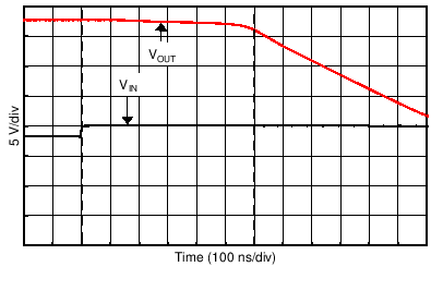
Positive Overload Recovery Figure 6-29
Negative Overload Recovery Figure 6-30
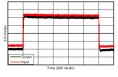
Small-Signal Step Response (10-mV Step) Figure 6-31, Figure 6-32
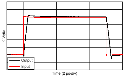
Large-Signal Step Response (10-V Step) Figure 6-33, Figure 6-34
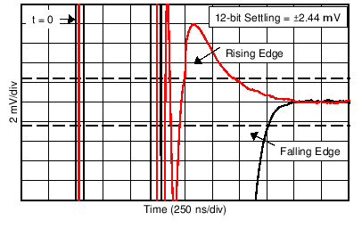
Settling Time Figure 6-35
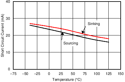
Short-Circuit Current vs Temperature Figure 6-36
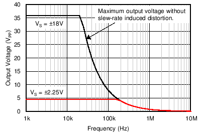
Maximum Output Voltage vs Frequency Figure 6-37
EMIRR vs Frequency Figure 6-38
GUID-8EA7410A-304C-44F6-A352-1F87DFD7231F-low.png
Figure 6-1 Offset Voltage Production Distribution
GUID-3170B0C8-BBA8-4474-B09C-E8AFE660BB4D-low.png
Figure 6-3 Input Bias Current Production Distribution
GUID-7873871B-8250-4918-A50B-616B153C87AB-low.png
5 Typical Units
Figure 6-5 Offset Voltage vs Temperature
GUID-7BD68DC6-8239-4287-818F-019E97E3A4DA-low.png
5 Typical Units
Figure 6-7 Offset Voltage vs Supply Voltage
GUID-69EC339E-ABD7-4995-9154-E9603C4C58B8-low.png
 
Figure 6-9 Closed-Loop Gain vs Frequency
GUID-38A39B82-95A0-4928-AA9A-5C40D52F1D39-low.png
 
Figure 6-11 Input Bias Current and Offset vs Temperature
GUID-00456637-CE31-43FA-9724-2E7148C59AE3-low.png
 
Figure 6-13 CMRR and PSRR vs Frequency
GUID-47A3CB87-E5C5-408B-8ECA-9E0170AAB2BF-low.png
 
Figure 6-15 PSRR vs Temperature
GUID-7FAB335D-2C79-4D4A-A65D-6144398C0518-low.png
 
Figure 6-17 Input Voltage Noise Spectral Density vs Frequency
GUID-BA10FF36-7A59-4968-B680-B6A5A0E5AAD8-low.png
f = 1 kHz BW = 90 kHz
Figure 6-19 THD+N vs Output Amplitude
GUID-E6B11BFA-60B5-44D4-B4F0-3C9B19852573-low.png
 
Figure 6-21 Quiescent Current vs Temperature
GUID-34100482-1B90-455E-BF5B-977A7106AC48-low.png
2-kΩ Load
Figure 6-23 Open-Loop Gain vs Temperature)
GUID-20201029-CA0I-VDGS-P1KR-1FGHF1BPFVQ7-low.png
VS = ±2.25 V
Figure 6-25 Open-Loop Gain vs Output Voltage Swing to Supply
GUID-20201029-CA0I-FP7N-WZGG-QC1C1LP2Z2HP-low.png
10-mV Step
Figure 6-27 Small-Signal Overshoot vs Capacitive Load
GUID-70238A29-8C66-4DBA-A88C-859B0637BC23-low.png
 
Figure 6-29 Positive Overload Recovery
GUID-270E758D-01B7-43A9-9F36-69A1515E1BCB-low.png
G = +1
Figure 6-31 Small-Signal Step Response (10-mV Step)
GUID-04AC774F-F48A-41DB-A68A-616B7E091E31-low.png
10-V Step G = –1
Figure 6-33 Large-Signal Step Response
GUID-DD777214-C679-41D7-A4A8-78B2ED87184A-low.png
12-bit settling on 10-V step = ±2.44 mV
Figure 6-35 Settling Time (10-V Step)
GUID-C606D4BF-68EB-4ED0-9A47-D2061A7C4E28-low.png
 
Figure 6-37 Maximum Output Voltage Amplitude vs Frequency
GUID-0AE8B514-19DF-4B32-89A8-B79790B55B61-low.png
Figure 6-2 Offset Voltage Drift Distribution From –40°C to +125°C
GUID-185813D9-1BDE-4F77-848A-6BA5509C9E67-low.png
Figure 6-4 Input Offset Current Production Distribution
GUID-26C6F2F3-56E4-4339-AE3F-10867FD503C6-low.png
5 Typical Units
Figure 6-6 Offset Voltage vs Common-Mode Voltage
GUID-FFE3587C-4969-4238-BE34-56AF6CA02B0B-low.png
 
Figure 6-8 Open-Loop Gain and Phase vs Frequency
GUID-3912ACB5-7FE7-4538-A350-20A7601DB195-low.png
 
Figure 6-10 Input Bias Current vs Common-Mode Voltage
GUID-50A7E51A-B109-4679-A2E9-E5B98FDE5890-low.png
 
Figure 6-12 Output Voltage Swing vs Output Current (Maximum Supply)
GUID-A674FF36-E347-4E6B-89EE-8354436C9D20-low.png
 
Figure 6-14 CMRR vs Temperature
GUID-9599568E-F9FC-4F7D-A5DA-04D97B4D9A5C-low.png
 
Figure 6-16 0.1-Hz to 10-Hz Voltage Noise
GUID-0266B3B9-D19A-4A23-93C0-CCAA72BC3F97-low.png
VOUT = 3.5 VRMS, BW = 90 kHz
Figure 6-18 THD+N Ratio vs Frequency
GUID-45902A9E-8512-4FC9-96D0-41BE82DAEB25-low.png
 
Figure 6-20 Quiescent Current vs Supply Voltage
GUID-E6F2093B-E549-4278-9F93-59D0C2AEF8C6-low.png
10-kΩ Load
Figure 6-22 Open-Loop Gain vs Temperature
GUID-20201029-CA0I-ZT3Z-7C4L-6V8KLN8H30FH-low.png
VS = ±18 V
Figure 6-24 Open-Loop Gain vs Output Voltage Swing to Supply
GUID-20201029-CA0I-Z6CP-SVBN-TJSF5WF0K8NF-low.png
 
Figure 6-26 Open-Loop Output Impedance vs Frequency
GUID-BD5B736A-D6D9-47C8-A6B2-CC27C70ACFB8-low.png
 
Figure 6-28 No Phase Reversal
GUID-3E70FE0E-BC2B-46F9-A4AD-3494EB58F075-low.png
 
Figure 6-30 Negative Overload Recovery
GUID-B5AAE211-EA20-4810-9B58-47D8121A3279-low.png
10-mV Step G = –1
Figure 6-32 Small-Signal Step Response
GUID-3C99ABAB-DD61-4BD1-A469-509FA50206D6-low.png
10-V Step G = +1
Figure 6-34 Large-Signal Step Response
GUID-9E456CCD-39CB-4C79-B8EA-3F45742C9D97-low.png
 
Figure 6-36 Short-Circuit Current vs Temperature
GUID-57B2FA91-16A0-46FC-BC5D-9323ED9CC481-low.png
PRF = –10 dBm
Figure 6-38 EMIRR vs Frequency