ZHCSE93 September   2015 OPA2171-EP

PRODUCTION DATA.  

  1. 特性
  2. 应用范围
  3. 说明
  4. 修订历史记录
  5. Pin Configuration and Functions
  6. Specifications
    1. 6.1 Absolute Maximum Ratings
    2. 6.2 ESD Ratings
    3. 6.3 Recommended Operating Conditions
    4. 6.4 Thermal Information
    5. 6.5 Electrical Characteristics
    6. 6.6 Typical Characteristics
  7. Detailed Description
    1. 7.1 Overview
    2. 7.2 Functional Block Diagram
    3. 7.3 Feature Description
      1. 7.3.1 Operating Characteristics
      2. 7.3.2 Phase-Reversal Protection
    4. 7.4 Device Functional Modes
      1. 7.4.1 Common-Mode Voltage Range
  8. Application and Implementation
    1. 8.1 Application Information
      1. 8.1.1 Electrical Overstress
    2. 8.2 Typical Application
      1. 8.2.1 Design Requirements
      2. 8.2.2 Detailed Design Procedure
        1. 8.2.2.1 Capacitive Load and Stability
      3. 8.2.3 Application Curve
  9. Power Supply Recommendations
  10. 10Layout
    1. 10.1 Layout Guidelines
    2. 10.2 Layout Example
  11. 11器件和文档支持
    1. 11.1 社区资源
    2. 11.2 商标
    3. 11.3 静电放电警告
    4. 11.4 Glossary
  12. 12机械、封装和可订购信息

封装选项

机械数据 (封装 | 引脚)
散热焊盘机械数据 (封装 | 引脚)
订购信息

5 Pin Configuration and Functions

DCU Package
8-Pin VSSOP
Top View
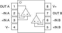
OPA2171-EP po_vssop-8_bos516.gif

Pin Functions

PIN I/O DESCRIPTION
NAME NO.
+IN A 3 I Noninverting input, channel A
+IN B 5 I Noninverting input, channel B
–IN A 2 I Inverting input, channel A
–IN B 6 I Inverting input, channel B
OUT A 1 O Output, channel A
OUT B 7 O Output, channel B
V+ 7 Positive (highest) power supply
V– 4 Negative (lowest) power supply